International Journal of Innovative Research in Science, Engineering and Technology
ISSN ONLINE(2319-8753)PRINT(2347-6710)
ISSN ONLINE(2319-8753)PRINT(2347-6710)
| M.Ananthi, A. Arul, R. Ramesh M.E. Applied Electronics, IFET college of Engg. Villupuram, Tamilnadu, India |
| Related article at Pubmed, Scholar Google |
Visit for more related articles at International Journal of Innovative Research in Science, Engineering and Technology
This paper presents the EMI reduction by the novel digital active technique used in a grid tied PV micro inverter module. The most commonly used passive EMI filter used for EMI mitigation in power converters comes at the expense of cost, size, weight power losses, and PCB real estate. DAEF is implemented with a grid tied photovoltaic micro inverter .the inverter stability is analyzed with the DAEF by the overall transfer function. The system compensation is designed based on the direct quadrant frame control technique
INTRODUCTION |
| The micro inverter architecture is used to connect the grid to convert the solar energy from PV panels and feed it to the grid with high efficiency and high power quality. The two main functions have done by the converter are as follows: |
| 1. Dc/ac power conversion. |
| 2. Tracking the maximum power delivered by the PV panel to maximize the energy throughput. |
| The fast dI/dt and dV/dt causes the fundamental and high frequency harmonics in the switching pulses of the inverter due to the non linear action of the switching semiconductor devices. |
| EMC compliance involves a series of measures to reduce conducted emission at the source. This can be done by diverting CM noise away from ground. Cost, size, and the space of the overall power inverter PCB. other EMI suppression technique |
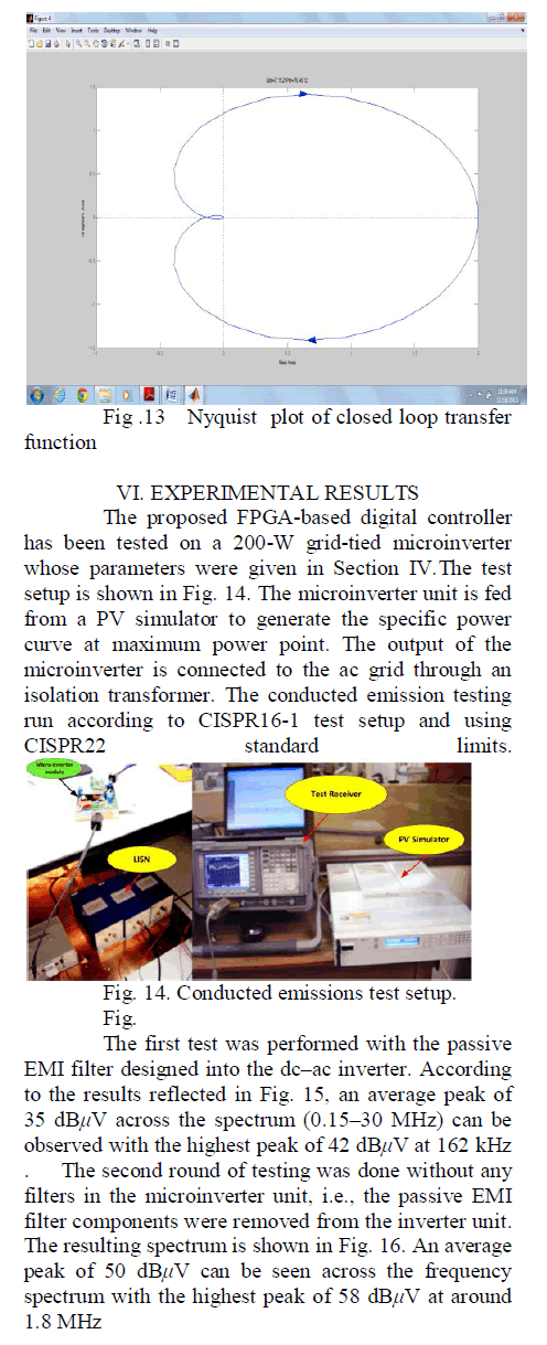
| The basic noise suppression technique is a passive EMI filter which gives the better performance but the Such as the spread spectrum frequency modulation and soft switching techniques has provide the less performance. Active analog EMI filters provides the low cost and ease of use .but it needs additional passive elements to noise attenuation of the spread spectrum .the deaf provides the best performance than |
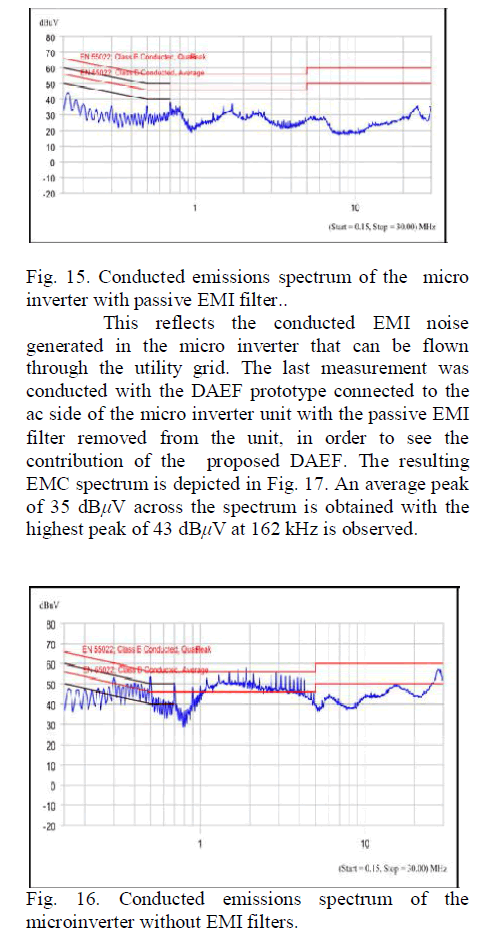
| The power circuit consists of micro inverter the previous EMI noise suppression techniques, used in the industrial applications, the DSP program to check the stability analysis of the inverter and FPGA program to the EMI control algorithm have been used in this paper. |
| This paper is partitioned as follows; in Section II, general descriptions of the micro inverters architecture and its inverter circuit including power conversion stages and controllers are presented. In Section III, the output inductor current control using a direct quadrature (DQ) reference frame control technique is explained. The open-loop transfer function (TF) of the micro inverter is derived to investigate the stability of the inverter in Section IV. Section V presents the controller design for micro inverter compensation and stability verification. Experimental results showing the performance of the DAEF in the micro inverter are illustrated in Section VI. Finally, a conclusion is given in Section VII. |
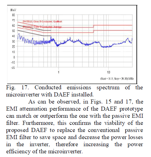
MICROINVERTER’S ARCHITECTURE AND CIRCUIT DESCRIPTION |
 |
| Two stages: dc/dc converter, and dc/ac converters. The functions. The first one is the boosting dc voltage to feed which is required by the grid .the second one is tracking the maximum power delivered by the photo voltaic panel to maximize the energy throughput. Then the second- stage dc/ac inverter converts the dc power into an instantaneous current and voltage suitable for the grid injection. |
| The digital control system consists of three main control functions: the maximum power point tracking (MPPT) control, the output inductor current Ilf control, and the EMI control. |
| Therefore, in the case of the two-stage micro inverter, a control algorithm is designed to keep the first stage of the inverter (dc/dc converter) operating at the maximum power, while the second - stage control algorithm is dedicated to regulate the instantaneous current or voltage to be injected into the grid. |
| DAEF CONTROLLER: |
| The rated current voltage of the power inverter depends on the size and losses of the filter. It is improved by the DAEF. It provides the maximum optimization of the inverter. The emulation of the incident CM noise signal in terms of amplitude and frequency is used for the DAEF. RF sensor senses the high frequency harmonics generated by the inverter, is used for the emulation process. The common mode interference signal is minimized by the digitally inverting the emulating signal. Then reconstruct the signal and inject back. It is generated by inverter switching circuitry. |
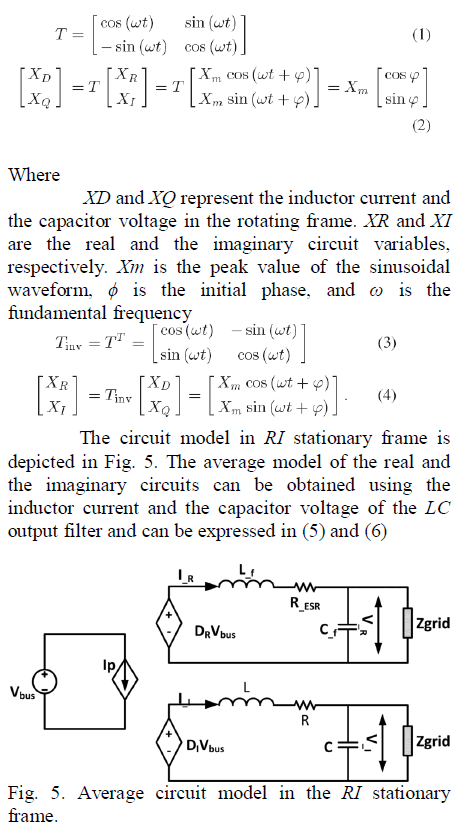
| The figure shows the digital active EMI filter with the grid side interface. The CM Noise voltage is sensed from the output of the inverter through RC high pass filter. It is input to the DAEF. it is sampled though high speed analog to digital converter. Then inverted using a binary inverter which output again converted by Digital to analog converter. The reconstructed signal is injected again back to the input lead of the power grid using a low pass filter which consist of capacitor and inductor. The low pass filter tuned to high frequency spectrum of the conducted emission standard. |
| Cinject is also used to prevent the ADC from being loaded by the power inverter. A high impedance inductor is located between the noise sensor and the grid as a decoupling network. In this process, only one control parameter is required by the digital processor in order to replicate the original sensed signal. |
| DC/DC two architecture consist of the |
| Output current controller |
| The DQ reference frame control technique is applied for controlling the instantaneous inductor current of single phase dc/ac inverter. In a DQ reference frame, the physical (Real) circuit, in conjunction with an “imaginary orthogonal circuit,” is transformed from the stationary frame to the DQ rotating frame so that the steady-state variables, voltage or current at the fundamental frequency, in the DQ frame become dc variables allowing the design of controller using design techniques developed for dc/dc converters. This design approach can achieve very high control gain which results in zero steady-state error at the fundamental frequency and better dynamic performance of the system. The following section provides a detailed analysis of the dc/ac inverter control technique. |
OUTPUT CURRENT CONTROL IN A DQ FRAME |
| The controller architecture using the DQ reference frame control technique of the two-stage micro inverter is depicted in Fig. 4. This controller diagram consists of three control blocks: MPPT controller, EMI controller, and the output inductor current controller. Only the last controller algorithm will be discussed in this section. |
| In Fig. 4, it can be seen that the real variables, which are the output inductor current Ilf and the grid voltage Vgrid are used to construct the imaginary circuit variables ID and IQ. These later are transformed into the DQ rotating frame using the real– imaginary (RI) stationary frame. The initial phase θ of the output voltage Vgrids locked using a phase-locked loop. The initial phase is used as a phase reference at the inverse transformation stage. The proportional and integral (PI) compensator is designed in the rotating frame with constant current reference ID ref and IQ ref . This generates the duty cycle control signals Duty_Q and Duty_D. The next step is the inverse transform of the duty cycle signals from DQ frame to RI stationary frame. Finally, the duty cycle signals of the imaginary circuit are decoupled from the RI stationary frame and only the duty ratio of the real circuit is applied to the dc/ac inverter stage. |
| The decoupling process is done using the initial phase reference to discard the imaginary function being a cos(ωt) or sin(ωt), orthogonal at 90âÃâæ phase shift, i.e., when the initial phase is a sin(ωt), the cos(ωt) of the imaginary circuit would be null, [cos(90âÃâæ)] = 0 and [sin(90âÃâæ)] = 1; hence, only the duty ratio of the real circuit is applied. Equations (1) and (2) provide the definition of the rotating transformation matrix from the stationary frame to DQ rotating frame. Equations (3) and (4) show the inverse transformation from the DQ rotating frame back to RI stationary frame |
 |
 |
 |
 |
 |
 |
 |
 |
 |
 |
 |
CONCLUSION |
| This paper proves the feasibility of replacing the conventional analog passive EMI filter by the DAEF in a solar grid-tied microinverter. In addition, the DAEF has been implemented concurrently with the inverter digital controller in an FPGA-based design. The TF of the micro inverter control system has been derived and analyzed using the DQ reference frame modeling technique. The stability of the micro inverter with the proposed digital controller has been verified and a compensator has been designed accordingly using the digital redesign approach. Compared with the conventional analog EMI suppression techniques, the size of the DAEF is not proportional to the power ratings of the converter; this means no bulky capacitor and oversized EMI choke need to be used. While providing matching or better EMI attenuation performance, significant reduction of the size, cost, and space of the overall power converter PCB can be achieved, hence further reducing power losses and increasing overall efficiency of the inverter. |
References |
|