Keywords
|
| IBC; Voltage multiplier module; PHEV |
INTRODUCTION
|
| Hybrid Electric vehicles are beingdeveloped by manufacturers to reduce the carbon dioxide emissions and to reduce the conventional fuel energy consumption.Recently, automotive manufacturers are developing plug-in hybrid electric vehicles (PHEV) which reduces the environmental pollution[1]. These vehicles have an AC/DC converter which supplies power from a commercial power supply to an on-board charger along with a DC/DC converter to supply power to its accessories. Because of the limitation in the charging time and restricted space, the DC/DC converters have to be designed efficiently[2]. |
| Interleaved Boost Converter (IBC) is employed in this work to step-up the input voltage that is being converted into DC by the rectifier. A two-phase interleaved structure is taken for this study because increasing the number of phases enhances the efficiency but the converter design becomes complex. Therefore, two-phase structure is preferred. Interleaving structure has two inductors connected in parallel and so the current path gets divided into two and the conduction loss can be reduced thus improving the overall efficiency η of the system[3]. |
| The duty ratio of the IBC is chosen to be 0.6,since it gives the maximum efficiency. The ripple reduction is a function of duty cycle. Because the two phases are combined at the output capacitor, effective ripple frequency is doubled, making ripple reduction much easier[4]. Since the output ripple is double the frequency of the individual phases and at a low rms current value, the size and the rating of the passive components that is being used can be reduced considerably. |
| Voltage multiplier cells are used to avoid narrow turn-off periods and to reduce the current ripple. Interleaved structure is used in the input side to distribute the current and voltage multiplier cells on the output side to achieve a high step-up gain. |
| A comparison between the topologies is done based on the various parameters like input current ripple, output voltage ripple, gain of the converter and the best one is chosen to be used along with the rectifier in the On-board battery charger. The main aim is to obtain a high gain converter with reduced input current ripple and reduced output voltage ripple. |
IBC TOPOLOGIES
|
| A. Basic Interleaved Boost Converter: |
| The conventional two phase boost converter consists of two single boost converters that are connected in parallel as shown in Fig 1. |
| Each switch is gated with a difference of 360/n where n is the number of phases and since here its two, the switches are gated with a phase difference of 1800.Using the IBC instead of the Conventional Boost Converter reduces the THD to about 40% in a PHEV[5]. |
| Operation: |
| Firstly when the device S1 is turned ON, the current in the inductor iL1 increases linearly. During this period energy is stored in the inductor L1. When S1 is turned OFF, diode D1 conducts and the stored energy in the inductor ramps down with a slope based on the difference between the input and output voltage. The inductor starts to discharge and transfer the current via the diode to the load. After half switching cycle of S1, S2 is also turned ON completing the same cycle of events. |
| The conversion ratio is a function of the duty cycle and the relation is as follows: |
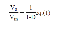 |
| where Vin is the input voltage, V0 is the output voltage and D is the duty ratio. |
| B. IBC with Diode-Capacitor multiplier: |
| The diode-capacitor multiplier cells helps to enlarge the voltage conversion ratio and to avoid extreme duty cycles. The voltage stress on the devices is less in this topology[6]. Here one stage of voltage multiplier cell is employed to reduce the complexity. The circuit diagram of the IBC with the diode-capacitor multiplier cells is as follows: |
| Operation : |
| The operation can be explained in four modes. |
| Mode 1: |
| At t = t0, switch S1 is ON, thus diode D0 is OFF. Switch S2 is also ON and thus D1 is OFF. Current increases linearly from its minimum value at t0 and current il2 increases linearly up to itsmaximum value at t1. iC1 is zero and uc1 is kept constant. |
| Mode 2: |
| The gating signal of switch S2 is removed; thus diode D1 is ON. Switch S1 is ON making diode D0 to turn OFF. Current il1 still increases linearly, inductor L2 charges C1 and then switch S2 is gated. |
| Mode 3: |
| Mode 3 operation is similar to that of mode 1. |
| Mode 4: |
| At t=t3, switch S1 is gated OFF, and diode D0 is turned ON. Switch S2 is kept ON and current il1 begins to decreases linearly through C1 which gets discharged. Whereas, current il2 still increases linearly.The time t4 is the ending of a switching cycle Ts. |
| The switching pattern of the DCM is as follows: |
| The conversion ratio here is given by : |
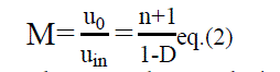 |
| where u0 and uin are the input and output voltages and n is the number of the multiplier cells. |
| C. IBC with Switched capacitor and Coupled inductor |
| The voltage multiplier module here consists of switched capacitors and coupled inductors. Using switched capacitor into an IBC makes the voltage gain to reduplicate, but the coupled inductor if not employed limits the voltage gain. Oppositely, if coupled inductors are used along with IBC the voltage gain is higher and adjustable but without switched capacitor the voltage gain is ordinary[7]. So, we integrate both into the circuit to obtain high step-up gain, high efficiency and low voltage stress. |
| The circuit diagram of this topology is as follows: |
| The coupled inductors extend the step-up conversion ratio whereas the switched capacitors offer extra voltage conversion ratio. The coupled inductors reduce the core loss in the circuit. The voltage conversion ratio here is given by: |
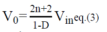 |
| where Vo and Vin are the input and output voltages and n is the number of the Voltage Multiplier Module(VMM). |
| Operation: |
| The operation of this circuit can be explained in eight modes: |
| Mode 1: |
| At time t=t0 , switch S2 remains in the ON state and S1 begins to turn ON. The coupled inductor release the stored energy to the output terminal through the forward diode Df2.The diodes Dc1, Dc2, Db1, Db2, and Df1 are reversed biased. The inductor L1 transfers energy to the secondary side of the coupled inductor. |
| Mode 2: |
| At t = t1, both of the power switches S1 and S2 remain in ON state, and all diodes are reversed biased. Both currents through leakage inductors L1 and L2 are increased linearly due to charging by input voltage source Vin. |
| Mode 3: |
| At t = t2, S1 ON state &S2 begins to turn off. The diodes Dc1, Db1, and Df2 are reversed biased.The diodes Dc1, Db1, and Df2 are reversed biased. The energy stored in the L2 is transferred to the secondary side of the coupled inductor. The current through the coupled inductor flows to output capacitor C3 through the flyback diode Df1. The voltage stress on the power switch S2 is clamped by the Cc1 which is equal to the output voltage. |
| Mode 4: |
| At t = t3, the current iDc2 has naturally decreased to zero due to the magnetizing current distribution, and hence, diode reverse recovery losses are alleviated and conduction losses are decreased. Both power switches and all diodes remain in previous states except the clamp diode Dc2 . |
| Mode 5: |
| At t = t4, the power switch S1 remains in ON state, and the other power switch S2 begins to turn on. The diodes Dc1, Dc2, Db1, Db2, and Df2 are reversed biased. The coupled inductor quickly releases the stored energy to the output terminal. Thus, the inductor L2 still transfers energy to the secondary side of coupled inductors. |
| Mode 6: |
| At t = t5, both of the power switches S1 and S2 remain in ON state, and all diodes are reversed biased. Both currents through inductors L1 and L2 are increased linearly due to charging by input voltage source Vin |
| Mode 7: |
| At t = t6, S2 is ON state, and S1 begins to turn off. The diodes Dc2, Db2 and Df1 are reverse biased. The voltage stress on power switch S1 is clamped by clamp capacitor Cc2 which equals the output voltage of the boost converter. The inductor L1 and capacitor Cc1 release energy to the output terminal. Thus the Vc1 obtains double output voltage of the boost converter. |
| Mode 8: |
| At t=t7, the current iDc1 has naturally decreased to zero and thus diode reverse recovery losses are alleviated. |
| D. Design Equations: The capacitors and inductors are designed using formulas given below: |
| ïÃâ÷ The value of the capacitor is got from: |
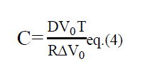 |
| where V0 is the output voltage |
| T is the time period |
| R is the resistance |
| ΔV0 is the ripple of the output voltage |
| D is the duty ratio |
| ïÃâç The value of the inductor is got from : |
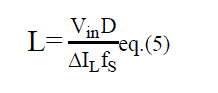 |
| where Vin is the input voltage |
| fs is the switching frequency |
| ΔIL is the ripple content in the Inductor |
| E. Simulation Results: |
| The three topologies are simulated in MATLAB with the following parameters constant for all the three topologies: |
| The simulation results of the three topologies are as follows: |
| An output voltage of 95V was obtained with the Interleaved Boost Converter. The fig5.andfig 6. shows the output voltage waveform and output voltage ripple waveform obtained with this topology. |
| The IBC with diode-capacitor multiplier produced an output voltage of about 176V. The output voltage waveform and the output voltage ripple waveform that was obtained in Matlab for this topology is shown in fig 7. and in fig 8. respectively. |
| The output voltage that was obtained with the IBC with switched capacitor and coupled inductor was 173V. The output waveform and the output voltage ripple waveform are represented in the fig 9. and fig 10. respectively. |
Inferences :
|
| The comparison of the three topologies have shown that though the output voltage ripple and input current ripple of the Diode-Capacitor multiplier is little higher compared to the other three topology, it is the optimum one and thus it is chosen for the battery charging application of PHEV. |
F. Conclusion :
|
| Various topologies of Voltage multiplier cells are simulated in the paper and comparison based on the various parameters are done. The IBC with the Diode-capacitor multiplier is proposed to be the best one to be used along with the rectifier for a PHEV with reduced input current and reduced output voltage ripple so that the size of the passive components like inductors and capacitors are reduced. A compact and efficient DC/DC converter thus can be developed. |
ACKNOWLEDGEMENT
|
| I am extremely thankful to Dr.R.Seyezhai, Associate Professor, EEEDepartment, my supervisor for providing me with her support, guidance and encouragement throughout the realization of this project. |
| I also thank Mr.Vigneshwaran of the CRF foundation for funding my project and supporting it financially. |
Tables at a glance
|
 |
|
| Table 1 |
Table 2 |
|
| |
Figures at a glance
|
 |
 |
 |
 |
 |
| Figure 1 |
Figure 2 |
Figure 3 |
Figure 4 |
Figure 5 |
|
 |
 |
 |
 |
 |
| Figure 6 |
Figure 7 |
Figure 8 |
Figure 9 |
Figure 10 |
|
References
|
- Masayoshi Hirota,TakeshiBaba,XiaoguangZheng, Kazuhiko NII, Shingo Ohashi,TakeshiAriyoshi and Hiroyuki Fujikawa,’Development ofNew AC/DC Converter for PHEVs and EVs’,Sei Technical Review · Number 73 · October 2011.
- Juan de Santiago, Hans Bernhoff, BoelEkergård, Sandra Eriksson, SenadFerhatovic, Rafael Waters, and Mats Leijon,’Electrical MotorDrivelines in Commercial All Electric Vehicles: a Review’, IEEE Transactions on Vehicular Technology,2012
- BurakAkin.’Comparison of Conventional and Interleaved PFC Boost Converters for Fast and Efficient Charge of Li-ion Batteries Used inElectrical Cars’, International Conference on Power and Energy Systems, Vol.13,2012.
- Wuhua Li, Yi Zhao, Yan Deng, and Xiangning He, ‘Interleaved Converter With Voltage Multiplier Cell for High Step-Up and High EfficiencyConversion’, IEEE Transactions on Power Electronics, Vol. 25, No. 9, September 2010
- WeerachatKhadmun and WanchaiSubsingha, ‘High Voltage Gain Interleaved DC Boost Converter application for Photovoltaic GenerationSystem’, ELSEVIER 10th Eco-Energy and Materials Science and Engineering,2013
- Luo-wei Zhou, Bin-xin Zhu, Quan-mingLuo, Si Chen, ‘Interleaved non-isolated high step-up DC/DC converter based on the diode–capacitormultiplier’, IET Power Electronics,Vol.7Iss . 2 June 2013
- Kuo-Ching Tseng and Chi-Chih Huang, ‘High Step-Up High-Efficiency Interleaved Converter with Voltage Multiplier Module for RenewableEnergy System’, IEEE Transactions on Industrial Electronics, Vol. 61, No. 3, March 2014
- Yi Zhao,Xin Xiang, ChushanLi,YunjieGu, WuhuaLi,Xiangning He, ’Single-Phase High Step-up Converter With Improved multiplierCellSuitable for Half-Bridge-Based PV Inverter System’,IEEE Transactions on Power Electronics, Vol. 29, No. 6, June 2014.
- WuhuaLi,Weichen Li, Xin Xiang, YihuaHu,Xiangning He, ‘High Step-Up Interleaved Converter With Built-In transformer Voltage MultiplierCells for Sustainable Energy Application’, IEEE Transactios on Power Electronics, Vol.29, No. 6, June 2014
- Murat Yilmaz and Philip T. Krein, ‘Review of Battery Charger Topologies, Charging Power Levels, and Infrastructure for Plug-In Electric andHybrid Vehicles’, IEEE Transactions on Power Electronics, Vol. 28, No. 5, May 2013
- Jae-Hyung Kim, Yong-Chae Jung, Su-Won Lee, Tae-WonLeez, and Chung-Yuen Wony, ‘Power Loss Analysis of Interleaved Soft SwitchingBoost Converter for Single-Phase PV-PCS’, Journal of Power Electronics, Vol. 10, No. 4, July 2010
- Marcos Prudente, Luciano L. Pfitscher, Gustavo Emmendoerfer, Eduardo F. Romaneli, and Roger Gules,’Voltage Multiplier Cells Applied toNon-Isolated DC–DC Converters’, IEEE Transactions on Power Electronics, Vol. 23, No. 2, March 2008.
- Ahmad Saudi Samosir, Taufiq, AbdJaafarShafie, Abdul HalimMohdYatim,’Simulation and Implementation of Interleaved Boost DC-DCConverter for Fuel Cell Applications’, International Journal of Power Electronics and Drive System (IJPEDS) ,Vol.1, No.2, December 2011.
- Haoyu Wang, SerkanDusmez, and AlirezaKhaligh,’Design Considerations for a Level-2 On-BoardPEV Charger Based on Interleaved BoostPFCand LLC Resonant Converters’,IEEE Transactions,2013
- Dr.K.Ravichandrudu, P.SumanPramod Kumar , M.Sailaja, M.Meena.’Power Factor Correction with Boost Rectifier’,International Journal ofAdvanced Research in Electrical, Electronics and Instrumentation Engineering,Vol. 2, Issue 7, July 2013
|