Keywords
|
| Distributed Generation, Quasi Z Source network, Clamped, Shoot through and Non-Shoot through states. |
INTRODUCTION
|
| More efforts are now being put into distributed power generation of renewable energy sources (RESs), such as photovoltaic (PV), wind power, and fuel cells, which are sustainable and environmental friendly. Practically, several distributed generations (DGs) consist of distributed power grid and further construct microgrid with local loads and managements. To ensure proper performance of the microgrid, DG is usually required to work in two modes: stand alone and grid connected. As an interface between RES and distributed power grid, the selection of power electronic converter becomes a hectic task. |
| There exist two traditional inverters: voltage-source (VSI) and current-source (CSI) inverters. In VSI, a constant voltage source acts as input to the inverter bridge. The constant voltage source is obtained by connecting a large capacitor across the DC source. In CSI, a constant current source acts as input to the inverter bridge. The constant current source is obtained by connecting a large inductor in series with the DC source. Typical inverters (VSI and CSI) have few disadvantages. They are listed below: |
| 1. Behaves as either boost or buck operation only. Thus the obtainable output voltage range is limited, either smaller or greater than the input voltage. |
| 2. Vulnerable to EMI noise and the devices gets damaged in either open or short circuit conditions. |
| 3. The combined system of DC-DC boost converter and the inverter has lower reliability. |
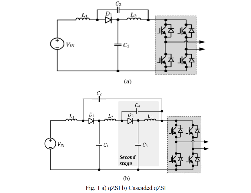
| To overcome these disadvantages a new concept was developed in year 2002 by Dr. F.Z. Peng. This involves combination of VSI and CSI to form a cross coupled network of two inductors and two capacitors, known as Impedance Network. Z-source inverter (ZSI) is known as a single-stage buck/boost inverter. With an impedance network coupling the inverter main circuit to the DC source, the ZSI achieves voltage buck/boost in one stage, without introducing more switching devices. Shoot-through state enables energy to be stored in inductors, which is released when at non-shoot through state, followed by the voltage boost feature. For the voltage-fed type ZSI (abbreviated as ZSI), voltage boost methods based on pulse width modulation (PWM) have been first investigated as simple boost control, maximum boost control, and maximum constant boost control. With a set of new topologies of the impedance networks, a class of quasi-Z-source inverter (qZSI) has been derived from the original ZSI and applied to DG applications. A voltage-fed qZSI (shown in Fig. 1(a)) was proposed for PV applications because of continuous input current and reduced passive component (capacitor) rating—capacitor voltage on C2 is much less than that on C1 during operating and this feature leads to lower manufacture cost. This paper discusses a method of performance improvement for the voltage-fed qZSI with continuous input current gained by the introduction of the cascaded quasi- Z-source network (qZS-network). The cascaded (two-stage) qZS-network is derived by the adding of one diode (D2), one inductor (L3), and two capacitors (C3 and C4) to the traditional qZSI, as shown in Fig. 1(b). This paper further proposes a new grid connected system which comprises of front end high step up conversion and 3-level level inverter. Front end high step up conversion comprises of a cascaded qZI, a high frequency isolation transformer and a voltage doubler rectifier (VDR) |
 |
PROPOSED BLOCK DIAGRAM
|
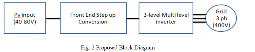
| The main focus of this paper is on the power converter (PC) for residential power systems. PCs are used to interconnect distributed energy sources producing low dc voltage, like solar panels (typically 40–80 V dc), to the residential loads (typically 3 × 400 Vac). Due to safety and dynamic performance requirements, the PC should be realized within the dc/dc/ac concept. This means that low voltage from the energy source first passes through the front-end step-up dc/dc converter with galvanic isolation afterwards, the output dc voltage is inverted with the three-phase inverter and filtered to comply with the imposed standards and requirements (second dc/ac stage). Our novel approach to the front-end stepup dc/dc converters provides a very high voltage gain. The block diagram of proposed grid connected system is shown in figure 2. |
 |
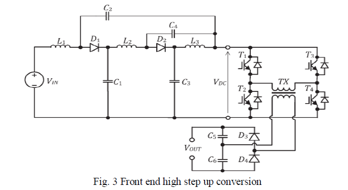 |
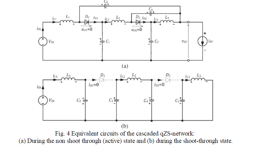
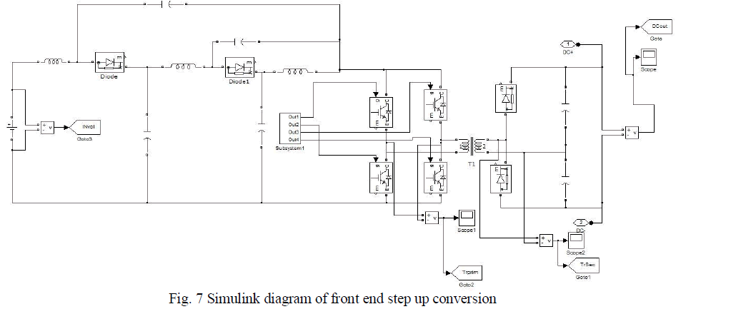
| The front end high step up conversion is shown in fig 3.The most important stage in step up conversion is cascaded qZSI. The equivalent circuits of cascaded qZSI in respective active and shoot through states are shown in fig 4. As the input voltage of PV varies, to regulate the varying input voltage, the front-end qZSI has two different operating modes: shoot-through and non-shoot through. In the non-shoot-through mode, the qZSI performs only the voltage buck function. This operation mode is typically used during light-load conditions, when the output voltage of a solar panel reaches its maximum. The inverter is controlled in the same manner as with the traditional VSI, utilizing only the active states when one and only one switch in each phase leg conducts. When the input voltage drops below some predefined value, the qZSI starts to operate in the shoot through mode. In order to boost the input voltage during this mode, a special switching state (the shoot-through state) is implemented in the pulse width modulation (PWM) inverter control. |
 |
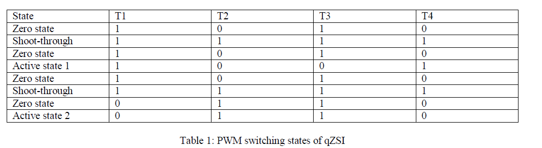
| The PWM switching states sequence presented in Table 1 shows that the upper and lower switches operate with different switching frequencies. The switching frequency of the upper switches (T1 and T3) in the shoot-through mode is equal to the fundamental frequency of the isolation transformer, while the switching frequency of the lower switches (T2 and T4) is three times higher than that of T1 and T3. |
 |
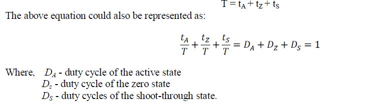
| The operating period of the PWM inverter during the shoot-through mode consists of an active state tA, a zero state tZ and a shoot-through state tS: |
 |
| Operation of voltage-doubler rectifier: |
| To reduce the turns ratio of the isolation transformer the voltage doubler rectifier (VDR) is implemented on the secondary side of the converter. In contrast to the traditional full-bridge rectifier, two diodes of one leg in the VDR topology are replaced by the capacitors. The operation principle of the VDR is explained in Fig. 5. |
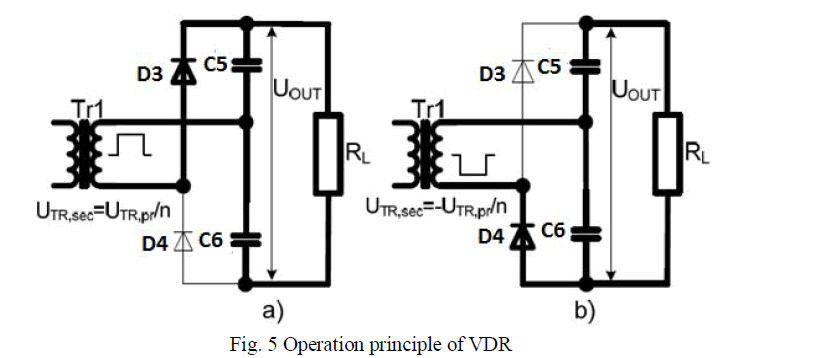 |
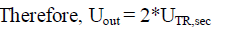
| During the positive half cycle, the capacitor C5 is charged through the diode D3 to the peak secondary voltage of the isolation transformer. During the negative half cycle the capacitor C6 is charged through diode D4. At every time instant the output voltage from this circuit will be the sum of the two capacitor voltages or twice the peak voltage of the secondary winding of the isolation transformer. |
 |
3-LEVEL MULTI LEVEL INVERTER
|
| Conventional 2-level PWM inverters generate high dv/dt and high frequency common mode voltages which deteriorate the performance of electrical appliances. Due to capacitor voltage unbalancing, neutral point potential also varies from zero. Recently, multilevel inverters have been found wide acceptability in medium and high voltage applications. Multilevel inverters have the advantage of producing high voltage-high power with improved power quality of the supply. It also eliminates the use of problematic series-parallel connections of switching devices. However, multilevel PWM inverters generate common mode voltages as in the case of conventional 2-level inverters. |
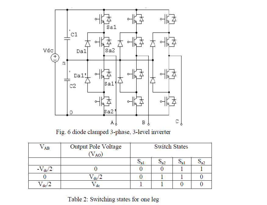
| Fig. 6 shows the very popular topological structure of diode clamped 3-phase, 3-level inverter. The switching states of the inverter are shown in Table 2 for one leg. It gives the output pole voltage VAO, output line voltage VAB and switch state. Switch state ‘1’ means ‘on’ and ‘0’ means ‘off’. This switching pattern can be achieved by means of different multilevel control strategies such as square wave switching, sine-triangle comparison method (SPWM), space vector modulation (SVM), selective harmonic elimination technique, hysteresis current control, sigma-delta modulation etc. Of these methods, sinusoidal pulse width modulation (SPWM) is the simple and cost effective method to implement. |
| The major advantages of the diode clamped inverter can be summarized as follows: |
| 1. When the number of levels is high enough, the harmonic content is significantly low to avoid the need of filters. |
| 2. Inverter efficiency is high because all devices are switched at the fundamental frequency. |
| 3. The control method is simple. |
| The major disadvantage of the diode clamped inverter can be summarized as follows: |
| 1. Excessive clamping diodes are required when the number of levels is high. |
 |
RESULT AND DISCUSSION
|
| The MATLAB-SIMULINK model of the qZSI-based DC/DC converter was developed and simulations made to analyze the proposed system. For all simulations the input voltage of the converter was set to 40-80V and the values of inductances in qZSI are 100μH and capacitances are 370μF. The turn’s ratio of isolation transformer is 1:3.75 with frequency 5 kHz. Capacitance values in VDR are 720μf. The input voltage, primary winding and secondary winding waveforms of isolation transformer and voltage profiles of the capacitors in qZS-network were measured. The whole model of step up conversion is shown in Fig 7. |
 |
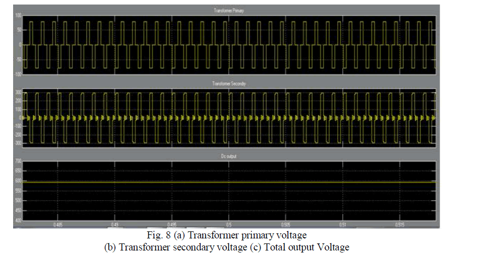
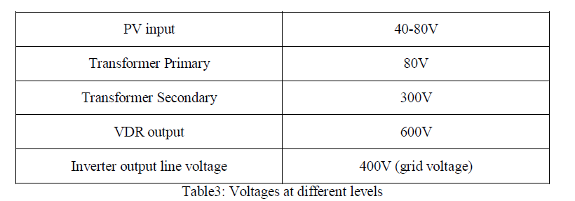
| The outputs measured from the power converter are shown in figure 8. Isolation transformer primary winding voltage is 80V and secondary winding voltage is 300V and the total voltage obtained from the VDR is 600V (i.e.., double of the secondary winding voltage) |
 |
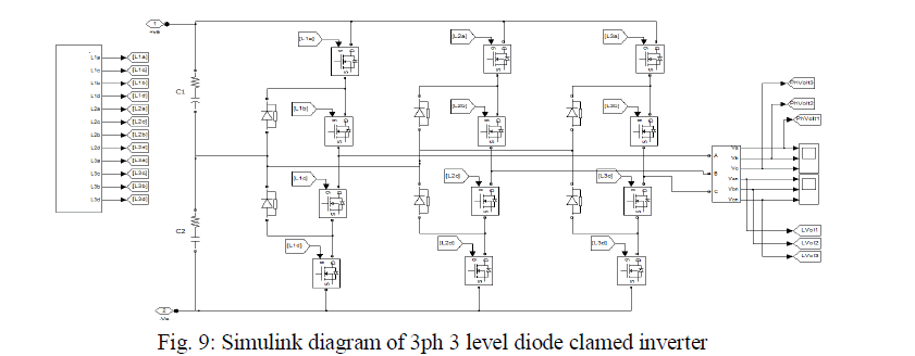
| The whole model of diode clamped 3-level inverter is shown in figure 9. The output (600V) of voltage doubler rectifier is given to the inverter to produce ac output voltage of 3 × 400 Vac. |
 |
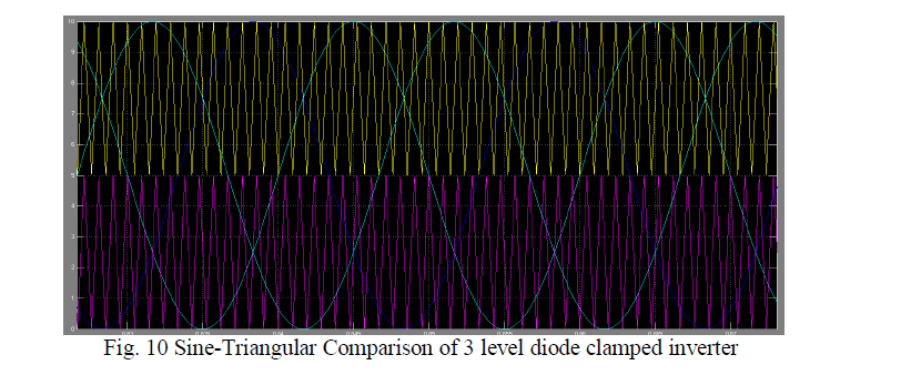
| One of the most straightforward methods of describing SPWM is to illustrate the intersection of a modulating signal (duty cycle) with triangle waveforms. Figure 10 demonstrates the sine-triangle method for a three-level inverter. The a , b ,c phase duty cycle is compared with two (n-1 in general) triangle waveforms. Where n is the level of the inverter. |
 |
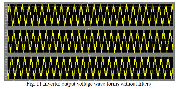
| Output line voltage waveform of the inverter is shown in figure 11. Generally an n-level inverter has n levels in phase voltage and 2n-1 levels in line voltage. So for 3-level inverter there will be 5-levels in line voltage as shown. |
 |
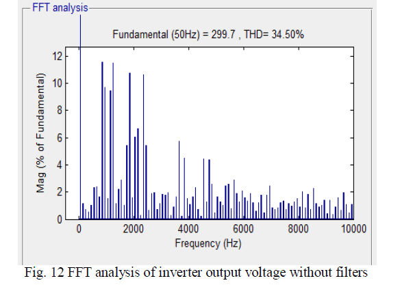 |
| The figure 12 shows the harmonic spectrum of inverter output voltage. By using the multi level inverters we can reduce the usage of bulky filters. By using more levels harmonics can be reduced drastically. Table 3 shows the voltages at different levels of the system. |
 |
| The results demonstrate that the proposed converter operates correctly, thus ensuring a ripple-free intermediate dc voltage VOUT. Also it is confirmed that the proposed converter ensures stable 3 × 400 Vacrms 50-Hz output voltage within the predefined input voltage. |
CONCLUSION
|
| This paper overcomes the problem with voltage source inverter by using Quasi Z Source network. To decrease the shoot through duty cycle at same voltage boost factor cascaded connection of qZSI is used and for further decreasing the shoot-through duty cycle the number of stages of the qZS-network could be increased. The usage of voltage doubler rectifier (VDR) results in less turns of ratio in isolation transformer. To decrease the stresses on the switches the PWM inverter is replaced by diode clamped multi level inverter. From results it is proven that the proposed front end high step up conversion has ripple free intermediate dc voltage and it is also confirmed that the proposed converter ensures stable 3 × 400 Vacrms 50-Hz output voltage within the predefined input voltage. |
ACKNOWLEDGMENT
|
| We express our sincere gratitude to Sir Mr. K. Narasimha Raju, Assoc. professor, EEE for encouraging and guiding us to undertake this paper work. We would like to thank Sir Mr. K. P. Prasad Rao, Asst. professor, EEE for his support and encouragement for this paper work. |
References
|
- J. Anderson and F. Z. Peng, “Four quasi-Z-source inverters,” in Proc. IEEE Power Electron. Spec. Conf., Jun. 15–19, 2008, pp. 2743–2749.
- Dmitri Vinnikov and Ryszard Strzelecki, “Step-Up DC/DC Converters With Cascaded Quasi-Z-Source Network”, in IEEE transactions onindustrial electronics, vol. 59, no. 10, pp. 3727 to 3736 october 2012.
- R. Strzelecki and M. Adamowicz, “Boost–buck inverters with cascaded qZ-type impedance networks,” Elect. Rev., vol. 86, no. 2, pp. 370–375,2010.
- D. Vinnikov and I. Roasto, “Quasi-Z-source-based isolated dc/dc converters for distributed power generation,” IEEE Trans. Ind. Electron., vol.58, no. 1, pp. 192–201, Jan. 2011.
- Jose Rodrihuez, J. Pontt, et. al, "A New Modulation Method to Reduce Common Mode Voltages in Multilevel Inverters," IEEE Trans.Industrial Electronics, vol. 51, no. 4, pp. 834-839, Aug. 2004.
- H. du Toit Mouton, "Naturtal Balancing of Three-Level Neutral Point Clamped PWM Inverter," IEEE Trans. Industrial Electronics, vol. 49, no.5, pp. 1017-1025, Oct 2002.
- M. H. Rashid, Power Electronics, 2nd ed. Englewood Cliffs, NJ: Prentice-Hall, 1993.
- F. Z. Peng, “Z-Source Inverter,” IEEE Transactions on Industry Applications, Vol. 39, No. 2, pp. 504-510, March/April 2003.
- Fang Z. Peng, X. Yuan, X. Fang, and Z. Qian, “Z-Source Inverter for Adjustable Speed Drives,” IEEE Power Electronics Letters, Vol. 1 No. 3,pp33-35, June 2003.
|