Keywords
|
| FPGA, Power Reduction, clock skew, dual Vdd. |
INTRODUCTION
|
| Field-Programmable Gate Arrays (FPGAs) are integrated circuits that can be programmed to implement any digital circuit. The main difference between FPGAs and conventional fixed logic implementations, such as Application Specific Integrated Circuits (ASICs), is that the designer/customer programs the FPGA on-site[1-3].For fixed logic, the designer must create a layout mask and send it to a foundry to be fabricated. Creating a layout is labor-intensive and requires expensive CAD tools and experienced engineers. Programmable switches controlled by configuration memory occupy a large area in the FPGA and add a significant amount of parasitic capacitance and resistance to the logic and routing resources. |
| Many studies have focused on reducing the speed and area overhead of FPGAs. Important advancements include clusterbased logic blocks[4], which improve speed by grouping the basic logic elements of the FPGA into clusters with faster local interconnect; embedded memories[5], which reduce the speed and area overhead for applications with storage requirements; and embedded ALUs[6], which reduce at the speed and area overhead for applications that perform arithmetic operations. As CMOS process technology scales down, the power density continues to increase due to higher chip operating frequencies, higher total interconnect capacitance per chip, and increasing leakage. Indeed, the International Technology Roadmap for semiconductors has identified low-power design techniques as a critical technology need[7]. |
POWER CONSUMPTION
|
| Due to the dramatic increase in portable and battery-operated applications, lower power consumption has become a necessity in order to prolong battery life. Power consumption is an important part of the equation determining the end product's size, weight, and efficiency. FPGAs are becoming more attractive for these applications due to their shorter product life cycle. FPGAs are programmable, so they allow product differentiation. Selecting an appropriate FPGA architecture is critical in achieving the best static and dynamic power consumption. As per we are dealing with Power optimization & reduction techniques. The two components to power consumption: static, dynamic. |
| Dynamic power is the power dissipated during active state due to switching activity of input signal [5].In other words, dynamic power dissipation is caused by the charging. Since an input can change without necessarily resulting in logic transition in the output, dynamic power can be dissipated even when an output does not change its logic state. The dynamic power dissipation is the result of charging and discharging parasitic capacitances. Dynamic power dissipation in a circuit is given as, |
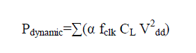 |
| Where C is the load capacitance, Vdd is the operating voltage,α is the activity factor of that net (the probability that net will switch in a given cycle) and f is the operating frequency of the node. The techniques to reduce Dynamic Power consumption are, Clock Gating, Power Gating, Improved switching activity, Glitch removal, Pipelining, Guarded Evaluation. |
LITERATURE SURVEY
|
| In previous work single voltage is applied to the whole circuit. The power consumed is high as both active and inactive blocks use the same supply voltage. This power consumption degrades the system performance and life time of portable application. In order to overcome this drawback, we propose dual Vdd technique along with controller device. As the switching power is quadratically related to the supply voltage, the power consumption is effectively reduced. |
| Power gating techniques can be classified into two types: coarse-grain power gating and fine-grain power gating. Low power FPGA architecture is generated with the use of fine grained Vdd control scheme called micro Vdd-hoping[8].The Vdd of each block is varied between the higher VDD and lower VDD spatially and temporalily to achieve low power. In fine grained power gating technique each lookup table have its own controller device. So the number of controllers used in fine grained technique is much larger than that of coarse grained technique. In this technique the controller device is always running. This results in large area and dynamic power overheads. Due to these overheads fine grained technique is less efficient than the coarse grained technique.[9] |
| In coarse-grain power gating, a large number of LUTs share a single sleep controller so the area and power overheads of the sleep controller are relatively small. |
PROPOSED METHOD
|
| Reducing the supply voltage (VDD) is an effective technique for reducing both dynamic and static power. Dynamic power has a quadratic dependency on supply voltage, while both sub-threshold leakage and gate leakage exhibit exponential dependencies on the supply voltage. However, reducing supply voltage also negatively affects circuit performance. A well-known technique to reap the benefits of voltage scaling without the performance penalty is the use of dual-VDD. The active blocks in the design operate on the normal VDD (or VDDH), while inactive blocks operate on a second supply rail with a lower voltage (or VDDL). While dual- VDD ICs have been successfully used in low-power ASICs and custom ICs [12], no commercial FPGA today uses multiple VDD for power reduction.The difficulty of designing a dual-VDD FPGA is that the optimal VDD assignment changes from one design to another. |
| Consequently, if logic blocks are statically determined to be operating at low or high VDD, the placement and routing algorithms need to be modified accordingly as in [11]. However, static assignment of VDD to the blocks may prevent the ability to reduce power consumption or to meet timing constraints for some designs. In contrast, the use of VDDprogrammability for each block helps to tune the number of high and low VDD blocks as desired by the application. In this approach, the challenge is in determining the VDD assignments to each block. Furthermore, positioning of the controller influences the ability to assign lower VDD to the routing blocks. In our programmable dual-VDD architecture (figure 3.1), the VDD of a circuit block is selected between VDDH and VDDL by using two high-VT transistors (supply transistors) connecting the block to the supplies. The state (ON/OFF) of each supply transistor is controlled by a configuration bit. |
SIMULATION RESULTS
|
| Comparison is made for various supply voltage scaling and it is found that power consumed by our Dual VDD technique is lesser than without controller device and also Idd is analyzed in Table4.1. |
CONCLUSION
|
| We have presented a dual-VDD FPGA architecture that provides significant power savings with minimal performance penalty. Variations of the VDD assignment and controller device were explored. The dynamic power was reduced around 45- 60%. Power supply network to support dual VDD or configurable VDD may introduce extra routing congestion. The total power reduction percentage for dual VDD FPGAs is significantly lower than the logic power reduction percentage. we will study how to reduce interconnect power by dual VDD in future |
Tables at a glance
|
 |
| Table 4.1 |
|
| |
Figures at a glance
|
 |
 |
 |
 |
| Figure 1 |
Figure 2 |
Figure 3 |
Figure 4 |
|
| |
References
|
- Xilinx, “Lowering power at 28 nm with Xilinx 7 Series FPGAs”, White paper WP389(v1.1.1),2012.
- Actel, “Dynamic power reduction in Flash FPGAs”, White paper, 2011.
- Xilinx (2011), “Power methodology guide,” White paper, UG786 (v13.1).
- V. Betz., J. Rose, and A. Marquardt, “Architecture and CAD for deep-submicron FPGAs”, Kulwer academic publishers,1999.
- S.J.E.Wilton, J. Rose, and Z.G. Vranesic, “Architecture of centralized field-configurable Programmable Gate Arrays(FPGA)”,pp.97-103,1995.
- S.Hong and S.S. Chin, “Reconfigurable embedded MAC core design for low-power coarse Grain FPGA”,IET Electronics Letters, Volume 39, Issue 7, pp. 606-608, 2003
- International Technology Roadmap for Semiconductors, 2011.
- Pooran singh,santosh kumar vishvakarma,”Device/circuit/Architectural Techniques for ultra low power FPGA design”,Microelectronics and solid state electronics,2013.
- Safeen Huda,Muntasir Mallick,Jason H.Anderson,”clock Gating Architecture for FPGA Power reduction”.
- A.Gayasen,K.Lee,N.Vijay Krishnan,M.Kandemi,M.J.Irwin,T.Tuan,”A Dual VDD Low power FPGA Architecture”,Pennsylvania state University.
- F.Li, D.Chen, L.He,and J.Cong.”Low-power FPGA using pre-Defined Dual-VDD/Dual-Vt Fabrics”.In Proceedings of ACM/SIGDA International Symposium on Field Programmable gate arrays,2004.
- M.Takahashi et.al.”A 60-mW MPEG4 Video Codec using Clustered Voltage Scaling With Variable Supply-voltage Scheme”,in IEEE Journal of solid state circuits,vol.33,No.11,Nov1998
|