International Journal of Innovative Research in Computer and Communication Engineering
ISSN ONLINE(2320-9801) PRINT (2320-9798)
ISSN ONLINE(2320-9801) PRINT (2320-9798)
Indumathi.M, A.Jeena Thankachan
|
| Related article at Pubmed, Scholar Google |
Visit for more related articles at International Journal of Innovative Research in Computer and Communication Engineering
Designing a new dual dynamic node hybrid flip-flop (DDFF) and low power 4/5 Counter was based on DDFF using FOOTED logic. The proposed designs eliminate the large capacitance present in the precharge node of several state-of-the-art designs by following a split dynamic node structure to separately drive the output pull-up and pull down transistors. The DDFF offers a power reduction of up to 62% and 48% compared to the conventional flipflops like Power PC 603 flip-flop and semi dynamic flip-flop. The aim of the DDFF-ELM is to reduce pipeline overhead. It presents an area, power, and speed efficient method to incorporate complex logic functions into the flipflop. The performance comparisons made in a 90 nm UMC process show a power reduction of 48% compared to the Semi dynamic flip-flop, with no degradation in speed performance. The leakage power and delay variations of various designs are compared with the proposed designs. The Footed logic is used to reduce power in the circuits. An efficient power reduction was obtained using footed logic and a single design was used for both counter which is called low power 4/5 counter.
KEYWORDS |
| Low power, Leakage current, Dual-Dynamic Flip Flop, high speed, Footed logic. |
I. INTRODUCTION |
| Power consumption plays major roll in Integrated circuits of VLSI design. In synchronous systems, high speed has been achieved using advanced pipelining techniques. In modern deep-pipelined architectures, pushing the speed further up demands a lower pipeline overhead. This overhead is the latency associated with the pipeline elements, such as the flip-flops and latches. |
| In the paper we introduce a new dual dynamic node hybrid flip-flop (DDFF) and low power 4/5 Counter was based on DDFF using FOOTED logic. The proposed designs eliminate the large capacitance present in the precharge node of several state-of-the-art designs by following a split dynamic node structure to separately drive the output pullup and pull down transistors. |
| The DDFF offers a power reduction of up to 62% and 48% compared to the conventional flip-flops like Power PC 603 flip-flop and semi dynamic flip-flop. The aim of the DDFF-ELM is to reduce pipeline overhead. It presents an area, power, and speed efficient method to incorporate complex logic functions into the flip-flop. The performance comparisons made in a 90 nm UMC process show a power reduction of 48% compared to the Semi dynamic flip-flop, with no degradation in speed performance. |
II. RELATED WORK |
| A. Semi Dynamic Flip Flop(SDFF) |
| Semi dynamic flip flop is fastest classic hybrid structure. They are purely dynamic designs as well as pseudo dynamic design, which has an internal precharge structure and static output. Dynamic frontend and static output. |
| Disadvantages |
| • Redundant data transitions, |
| • Not efficient for power consumption because of large clock and large precharge capacitance, |
| • High power consumption devices, |
| • Area is also high. |
| B. Cross Charge Control Flip Flop(XCFF) |
| A low power and high-speed flip-flop named Cross Charge control Flip-Flop (XCFF). It has two dynamic nodes driving output transistors separately. The minimum power-delay product of the XCFF is 48% smaller than that of CMOS flip flop and 20% smaller than that of the semi dynamic Flip-Flop (SDFF). Charge sharing is uncontrollable when complex functions are embedded is the disadvantage. |
| C. Conditional Data Mapping Flip Flop(CDMFF) |
| A new family of low power and high-performance flip flops, namely conditional data mapping flip flops (CDMFFs), which reduce their dynamic power by mapping their inputs to a configuration that eliminates redundant internal transitions.The conditional data mapping flip flop (CDMFF) is one of the most efficient which uses an output feedback structure to conditionally feed the data to the flip flop. This reduces overall power dissipation by eliminating unwanted transitions when a redundant event is predicted.c |
| D. Power PC 603 Flip Flop |
| PowerPC 603 is one of the most efficient classic static structures. The PowerPC 603 was based on master slave latch. They dissipate comparatively lower power and have a low clock-to-output (CLK-Q) delay. In a synchronous system, the delay overhead associated with the latching elements is expressed by the data to output (D-Q) delay rather than CLK-Q delay. It has advantages of having low power keeper structure and low latency direct path. Disadvantage of large data to output delay during large setup time. |
| E. Dual Dynamic Flip-Flop (DDFF) |
| In DDFF architecture Node X1 is pseudo-dynamic, with a weak inverter acting as a keeper, whereas, compared to the XCFF, in the new architecture nodeX2 is purely dynamic. An unconditional shutoff mechanism is provided at the frontend instead of the conditional one in XCFF. The operation of the flip-flop can be divided into two phases: |
| 1) The evaluation phase, when CLK is high, and |
| 2) The precharge phase, when CLK is low. |
| Evaluation phase |
| ïÃÆÃË When Clk=1 and D=1, x1 discharged , it switches the INV1-2 (pair) and X1B=1 & QB discharge QB=0&Q=1. |
| ïÃÆÃË X1=0 will maintain throughout the evaluation phase. |
| ïÃÆÃË Clk=0->1 and D=0 X1=1 X2=0, QB=1 &Q=0. |
| Precharge phase |
| ïÃÆÃË CLK =0 and D=1 X1=1 it switches the state of INV1-2 and X2 is in inactive state. It store the charge dynamically. |
| ïÃÆÃË QB maintain previous state QB=0 and Q=1. |
| ïÃÆÃË CLK =0,D=0 it will remain previous state Q=0 and QB=1. |
III. PROPOSED WORK |
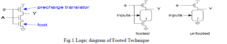
| A. Footed Logic |
| An NMOS transistor is introduced in the circuit whose gate is shorted with its drain and connected to the source of the NMOS (before) clock transistor. The source of NMOS transistor is connected to gate. When input is low then dynamic node is always high and output is kept low regardless of operating phase. |
 |
| B. High-Speed Divide 4by5 Counter |
| Most divide-by-128/129 dual-modulus prescalers consist of a synchronous divide 4by5 counter as the first (high-frequency) stage, followed by a chain of toggle flip-flops (TFFs), which forms an asynchronous divide-by-32 counter as the second (low-frequency) stage. The operating speed of prescalers is mainly limited by that of the divideby- 4/5 counter. |
| There is a clock preprocessor(CP) and also two TFFs in the circuit. The clock preprocessor consists of a „half transparentâÃâ¬ÃŸ (HT) register in the front, and a domino CMOS logic in the rear. The HT register in its register mode (with a „0âÃâ¬ÃŸ input) is extremely fast, nearly one inverter delay is required. In its transparent mode (with a „1âÃâ¬ÃŸ input), the inverse data directly returns to the input of the precharged stage (becoming „0âÃâ¬ÃŸ) so that the output signal is allowed to delay a period of the input signal. If MC is set to „OâÃâ¬ÃŸ, then MCx is always „lâÃâ¬ÃŸ, and this domino gate is used as the buffer stage of the two-stage inverter and directly transports the signal to the next stage (TFF). The state in the HT register is not effected since its input CKx is the inverse of clock signal „id. |
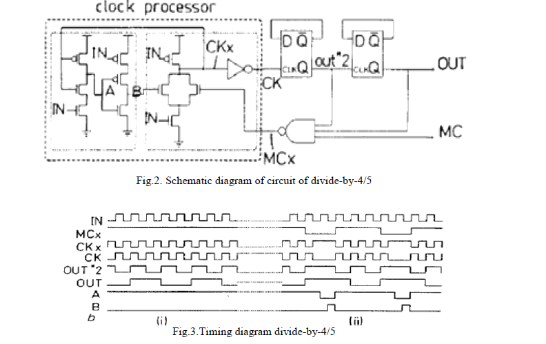 |
| (i) waveforms on divided-by-4 circuit (mc = 0) |
| (ii) waveforms on divided-by-5 circuit (mc = 1) |
IV. SIMULATION RESULTS |
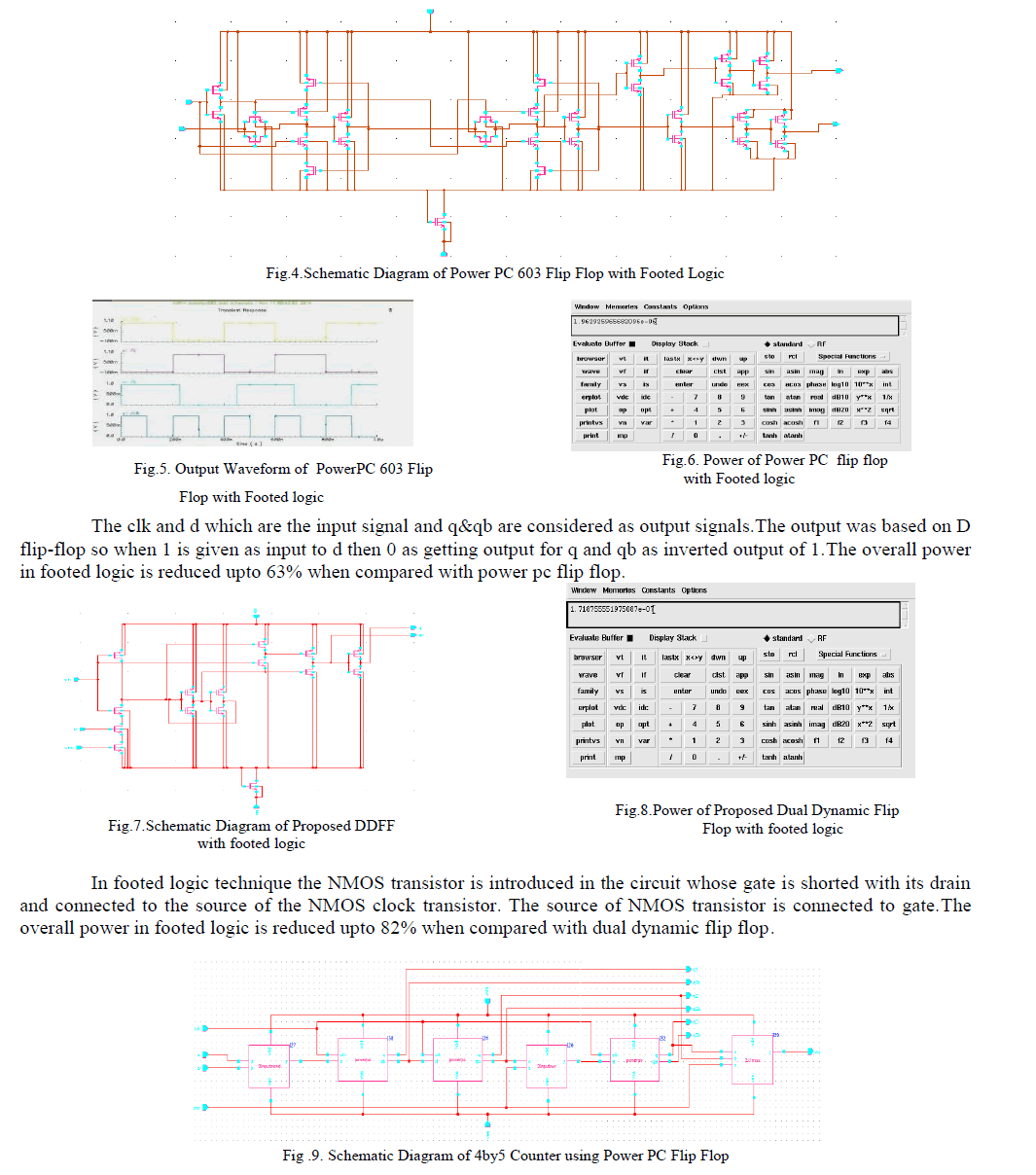 |
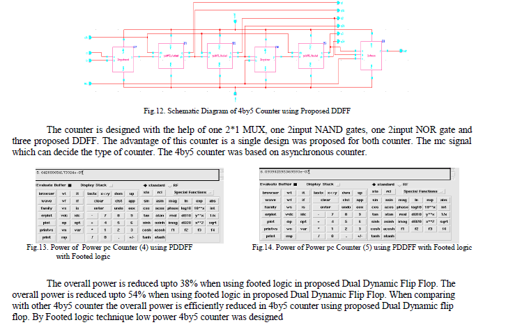
| The counter was designed with the help of one 2*1 MUX, one 2input NAND gates, one 2input NOR gate and three power pc flip-flop. The advantage of this counter is a single design was proposed for both counter. The 4by5 counter was based on asynchronous counter it does not require clock pulse for every individual flip flop.In asynchronous counter communication in which data can be transmitted rather than in a steady steam. |
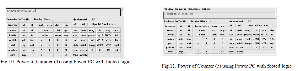 |
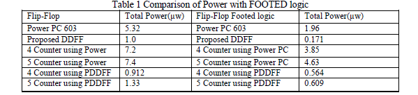
| The power is reduced upto 87% when using footed logic in power pc flip flop in 4by5 counter(4 counter). The power is reduced upto 82% when using footed logic in power pc flip flop in 4by5 counter(5 counter). The power consumption in dual dynamic flip flop was better so its greater to consider for designing 4by5 counter using proposed dual dynamic flip flop. We calculate the power of 4by5 counter when the mc signal is 0 so that counter act as 4 counter and then when mc signal is 1 counter act as 5 counter. |
 |
 |
| The comparison table of overall power produced using various flip flop and flip flop with footed logic is compared and given in above table. It was concluded that the 4by5 counter has low power when it is designed using Proposed Dual Dynamic Flip Flop. |
V. CONCLUSION |
| A new low power DDFF and a low power 4by5 counter is designed. The proposed DDFF eliminates the redundant power dissipation present in the XCFF. A comparison of the proposed flip-flop with the conventional flip flops with Footed logic showed that it exhibits lower power dissipation along with comparable speed performances. A new divide 4by5 circuit without pass gates is adopted for the high-speed prescaler. The experimental results of the prescaler have demonstrated its ability to operate up to 1.1 1 GHz with low power consumption .The diode-footed domino circuit design style and demonstrated that the technique is leakage-tolerant, achieves highperformance and low power compared to the conventional domino styles, and is suitable for scaled CMOS technologies. Power is reduced using low power techniques such as FOOTED DIODE and MTCMOS. The power produced by 4/5 counter using proposed Dual Dynamic Flip Flop was reduced upto 38% and 54% for 4 counter and 5 counter respectively. |
References |
|