International Journal of Advanced Research in Electrical, Electronics and Instrumentation Engineering
ISSN ONLINE(2278-8875) PRINT (2320-3765)
ISSN ONLINE(2278-8875) PRINT (2320-3765)
M.Kanagarasu, S.Nageswari, Jebasalma
|
| Related article at Pubmed, Scholar Google |
Visit for more related articles at International Journal of Advanced Research in Electrical, Electronics and Instrumentation Engineering
It is proposed to analyze the performance of solar powered multilevel Neutral Point Clamped (NPC) inverter in low modulation index region using carrier based pulse width modulation (PWM). The solar panel act as variable DC voltage source input to the inverter. Using advanced carrier based dipolar PWM technique is used to have increased number of output voltage levels and reduced THD in low modulation index region.Simulation and measurement results using MATLAB/SIMULINK illustrate the advantage of the proposed PWM.
Index Terms |
| NPC inverter, unipolar PWM and dipolar PWM, low modulation index. |
INTRODUCTION |
| In recent years, the use of renewable energy resources instead of pollutant fossil fuels and other forms has increased. Photo Voltaic (PV) generation is becoming increasingly important as a renewable resource since it does not cause in fuel costs, pollution, maintenance, and emitting noise compared with other alternatives used in power applications. Higher power equipment’s require higher voltages, which limit the maximum DC voltage level. Therefore a new family of multilevel inverters has emerged as the solution for solar applications, as the PV array is directly connected to each level of the DC link multilevel power conversion technology is a very rapidly growing area of power electronics with good potential for further development. The most attractive applications of this technology are in the medium- to high-voltage range (2-13 kV), and include motor drives, power distribution, power quality and power conditioning applications. |
| Multilevel inverters are being used for high voltage and high power industrial applications [1]. In high power drives application, it is troublesome to connect only one power semiconductor switch directly. As a result, multilevel structure has been introduced as an alternative in high power and medium voltage situations. The most popular topology used in medium voltage applications is the three level diode clamped converter also known as neutral point clamped (NPC) converter topology [2]. Due to serial power switch connection of devices, the device voltage stress is reduced. This topology produces multilevel line voltages hence the input voltage harmonics are reduced. |
| In general, use of three level NPC inverter to an industrial application has the following advantages |
| Distortion of the current and voltage waveforms can be effectively reduced, because of the increase in levels of the output voltage pulse trains. |
| Switching device with relatively lower blocking voltage such as an IGBT can be used for the main circuit, because a switching device voltage can be decreased approximately half that of the two level inverter. |
| This topology requires high speed clamping diodes that must be able to carry full load and are subject to severe reverse recovery stress. Although measures to alleviate this problem can be applied, this remains a serious consideration. |
| Lower loss in the main circuit of the inverter can be expected, because of the decrease in switching device voltage |
Low Modulation index problem |
| Pulse-width modulation (PWM) strategies are required for switching the devices in a VSI appropriately to generate variable voltage, variable frequency. Typical desired features of a PWM technique are low THD, low switching loss, less computational and simple implementation. However in low modulation index region PWM inverter outputs have undesirable effects, such as reduced output line to line voltage levels, increased THD and uncontrollability. |
| In this work, two modulation schemes such as carrier based unipolar PWM and carrier based dipolar PWM are analyzed. Proper comparisons of the harmonic performance of the PWM methods are carried out. This work mainly considers of utilizing all level of the inverter output voltage and to reduced THD at low modulation index region. |
PWM TECHNIQUES |
| There are several PWM methods used to control the output voltage of inverters. |
A. Unipolar Pulse Width Modulation (PWM) |
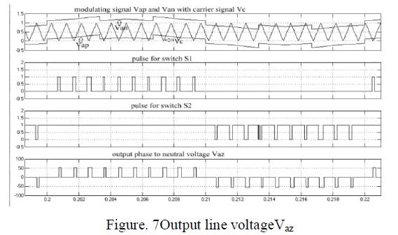
| In the unipolar mode, two sinusoidal signals with a single carrier are used. One of the sine signal starts at zero position called positive signal (Vap) and another one starts at one called negative signal (Van). Comparison of Vap signal and carrier signal provide pulses to the switch S1 in phase A leg and the complementary pulse is given to the switch S3 in thesameleg, comparison of Van signal and carrier signal generate pulses for switch S2 of NPC inverter shown in Figure. 6 and the inverted pulse is given to switch S4. |
| The general schematic of three-level unipolar PWM is shown in Figure.1 from the commanded voltages V∗k(k = a, b, c), two auxiliary commands V*kpand V*knare derived. |
<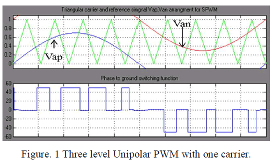 |
| In unipolar modulation mode, only one capacitor is connected to the output per half-cycle of the fundamental frequency. This modulation mode is preferred at high output frequencies. |
B.Dipolar Pulse Width Modulation (PWM) |
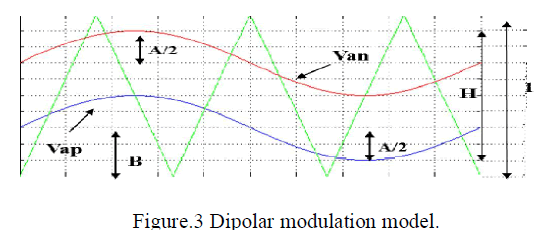
| Dipolar PWM method uses a single triangular carrier wave, and two sinusoidal modulating signals shown in Figure. 3 Dipolar PWM is formed by the splitting of single sinusoidal signal into two. This splitting is implemented to break each commutation between outer levels +Vd/2 and –Vd/2, by forcing a passage of PWM waveform through the intermediate zero level. Width of the zero level pulse corresponds to the period while the carrier is comprised between the two modulating waves. |
| Modulation index (ma) and frequency ratio (mf) are defined for unipolar PWM method. Calculation of distance between the modulating waves a parameter H is used which is defined as the ratio of vertical distance between the minimum of the positive sinusoidal reference signal (Vap) and maximum of the negative sinusoidal reference signal (Van) to the amplitude of the carrier wave. During H=ma, dipolar modulation is similar to bipolar one. |
< |
PROPOSED SYSTEM |
A. Block Diagram of Proposed System |
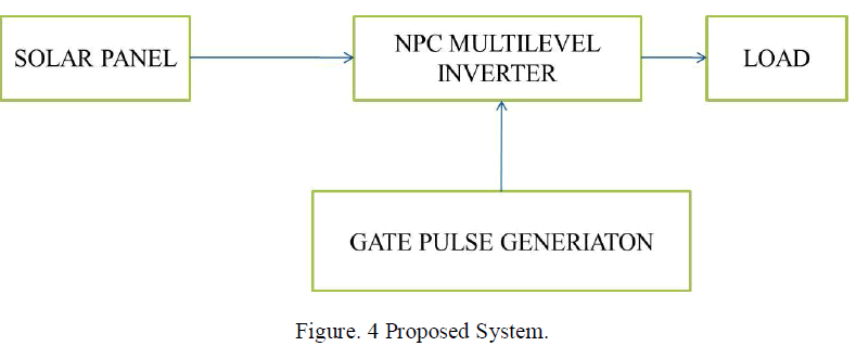
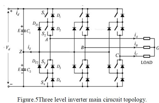
| Solar panel have a number of solar cell, a solar cell is a semiconducting device that absorbs light radiation and converts it in to electrical energy, that electrical energy source is given to the input of multilevel inverter. The ability of the NPC topology to generate better output performance in terms of harmonic content prompted the development of multilevel topology to higher number of voltage levels using the similar principle of clamping the intermittent levels with diodes. Such multilevel structures are known as ‘diode clamped multilevel inverters’. As shown in Figure. 5, |
< |
| Am-level diode clamped inverter requires (m-1) series-connected capacitors in the DC-link, where each capacitor is charged to an equal potential. For a DC-link voltage, Vd, the voltage level of each capacitor is Vd/2 for a NPC. Due to the connections of the clamping diodes, the voltage stress across the switching devices is limited to one capacitor voltage level. Therefore, by increasing the number of voltage levels, the voltage stress across the semiconductor switches in this multilevel structure can be reduced significantly. |
< |
B. Carrier Based PWM Technique for Three Level Inverter |
| Any balanced three-phase reference voltage can be represented by a space vector on the diagram. A typical space-vector modulator uses the nearest three states (nodes of the triangle containing the vector) to approximate the desired voltage vector. During each switching period, the triangle is traversed back and forth once. The switching sequence and dwell times in each state are determined by requiring volt-seconds produced by switching state vectors equal to that of the reference vector. Note that dwell time here is defined as the time spent in a given switching state and should not be confused with dead time which pertains to the lockout time between switches on the same phase leg to avoid shoot through[14]-[16]. The minimum dwell time should be greater than the nominal dead time. Space vector produced by the hybrid multilevel inverter the definition of space vector is |
< |
| Large vectors and zero vectors do not produce any NP current, NP and hence do not affect the NP voltage. Medium and small vectors affect the NP balance, but only the small vectors come in pairs.Both vectors in a pair produce the same lineto- line voltage, but produce the NP current in opposite directions. The first logical step to establish their relation is to determine the phase voltage generated as a result of space-vector modulation. |
C. Dipolar PWM Pulse Generation |
| Dipolar PWM method uses two modulation wave signals, the positive one Vap, to control positive and negative one van, to control negative output voltage pulse trains as shown in Figure. 3. The amplitude and the base line shifts of these modulation waves are equal to half of the modulation index m and bias B, respectively[12]. These positive side and negative side modulation waves can be expressed as follows, |
<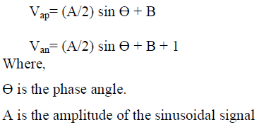 |
| B is the Bias |
| The value of B must always be less than 0.5 for this method to be successful. and the value of A must be less than 1.Minimum Bias value is calculated as the product of Vd and minimum on time of the switch and frequency of the triangular carrier signal[4]-[8]. |
| To achieve dipolar operation upto modulation index (ma)=0.4 bias B value must be greater than 0.2 . To achieve full level of output as the linear range bias B value is chosen as 0.4 [5]. |
| Condition For Common Mode Injection For CenteredModulator: |
<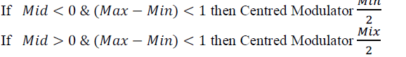 |
| To improve the THD in lower modulation index region, to obtain the controllability and to have effective utilization of all levels in low modulation index region, carrier based - dipolar PWM is used.Above TableI summarizes the common-mode injection function required to achieve a centered sine-triangle three-level modulation. Based on the algorithm, a modulator was developed and tested on a real-time simulator. |
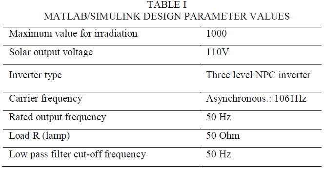
D. Circuit Specifications |
| Parameters chosen for simulation of unipolar SPWM and dipolar PWM are tabulated in Table. I. |
< |
E. Gate Pulse Generation |
<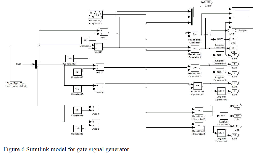 |
| The modulating signal is compared with the triangular carrier signal to generate the 12 switching pulses as shown in Figure.6. |
SIMULATION RESULTS |
a. Output for carrier based unipolar-PWM at modulation index (Ma=0.27). |
< |
<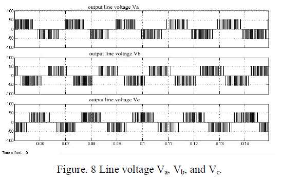 |
| From Figure. 7 shows line to neutral voltage Vaz and Figure. 8 shows line voltage of unipolar PWM have only three levels of output for ma=0.27. |
<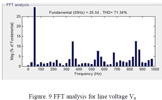 |
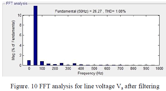
| The FFT analysisshown in Figure. 9 fundamental voltage with 25.54 V and before filtering THD =71.34 %, after filtering THD = 1.08 % for Ma=0.27 as show inFigure. 10. |
< |
b. Output for carrier based dipolar-PWM at modulation index (Ma=0.27) |
<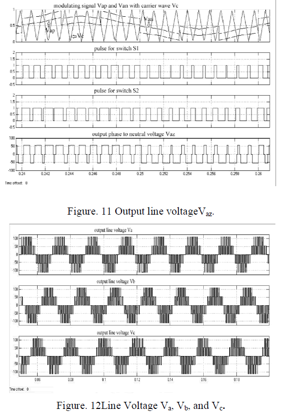 |
| Figure. 11 shows line to neutral voltage Vaz and Figure.12 shows line voltage of dipolar PWM have only three five level of output for low modulation ma=0.27. |
<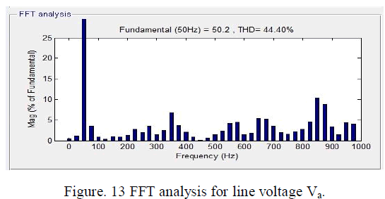 |
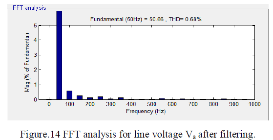
| From the FFT spectrum shown in Figure 13 fundamental voltage with 50.2 V and before filtering THD =44.4 %, after filtering THD = 0.68 % for Ma=0.27 as show inFigure 14. |
< |
c. Result comparison |
| Table IV shows the performance comparison of the proposed carrier based unipolar PWM and Dipolar PWM. The comparison results show that the proposed carrier based –Asynchronous Dipolar PWM improves the levels up to 0.15 modulation index and THD values (after filtering) are reduced significantly than the unipolar PWM methods. |
<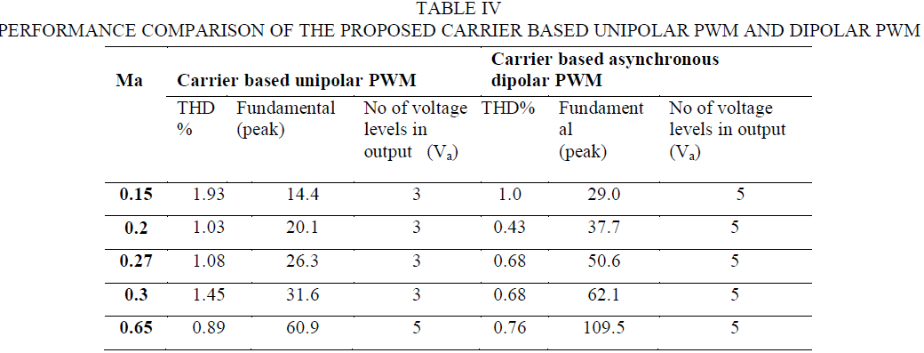 |
CONCLUSION |
| The proposed carrier based dipolar PWM is applied to solar powered multilevel NPC inverter in low modulation index range. The proposed system the number of levels in the output voltage is increased. Low modulation index problems such as reduced number of levels, minimum pulse width limitation and higher THD are given attention.Carrier based unipolar PWM and dipolar PWM are simulated. The comparison results are produced. By comparing the results, dipolar PWM produced more number of levels in the output line voltage and less THD compared to unipolar PWM. Dipolar PWM solves the pulse width limitations and uncontrollability problems. |
| The fundamental voltage of carrier based dipolar PWM is more compared to unipolar PWM and also THD of carrier based dipolar PWM is low compared to unipolar PWM. |
References |
|