Research & Reviews: Journal of Material Sciences
ISSN:2321-6212
ISSN:2321-6212
Ktifa S*, Ezzaouia H
Photovoltaic Laboratory, Research and Technology Centre of Energy, Borj-Cedria Science and Technology, Tunisia
Received date: 25/02/2016; Accepted date: 31/03/2016; Published date: 07/04/2016
Visit for more related articles at Research & Reviews: Journal of Material Sciences
In this paper we have studied the thermal properties of silicon thin films deposited by plasma enhancement chemical vapor deposition (PECVD) on porous aluminum using the phothermal deflection technique (PTD). The aim of this work is to investigate the influence of anodisation current (between 200 to 400 mV) on the thermal conductivity of samples. We present a computational model to determine the thermal conductivity K. The coincidences between the experimental and theoretical curves permit to deduce the values of thermal conductivity with a good accuracy. In fact, it was found that K decrease with the anodisation current.
Porous aluminium; Photothermal deflection thechnique (PTD); Thermal conductivity
Porous ceramic materials are used in several applications in many engineering and industrial fields namely filters and membranes, catalyst for biomaterials, cell electrodes, and acoustically bulk media. Porous anodic alumina films is an interesting material [1] for nanotechnology applications because of its unusual properties compared to the bulk counterparts [2]. Many works have been published relative to the deposition of porous aluminum films [3]. Different methods of film growth were used, as for example reactive sputtering [4] and low pressure metal-organic chemical vapor deposition [5]. Thermal conductivity of ceramics is of general interest, since it may significantly influence other properties such as thermal shock resistance and may exhibit certain features, in particular porosity dependence, analogous to other properties [6]. The prediction of their thermal properties by analytical or computer calculation is therefore of strong interest [7]. In this work we demonstrate the capability to grow porous aluminum layers (PAL) by electrochemical anodisation method; the anodizing process was done by varying the anodizing voltage between 250 to 400 mV. A crystalline silicone films are deposited on the PAL by a PECVD technique. We present a computational model to determine the thermal conductivity K using the photothermal deflection technique (PTD).
High-purity aluminum foil (99.997%), 0.25mm thick was used as a starting material. The cleaned samples were anodized during 25 min in a solution of diluted sulfuric acid with 66.66% H2SO4 and 33.33% H2O2 at room temperature and with five different anodization currents (250 mA, 300 mA, 350mA and 400 mA). On the surface, nc-Si films were deposited by PECVD technique [8] at 50°C using a gas mixture of silane and H2 at a total pressure of 0.5 mTorr.
The experimental device [9] is shown in Figure 1. The PTD is a sensitive optical tool for material analysis]. When a sample is irradiated with modulated and monochromatic beam radiation, the absorbed energy is converted into heat through different relaxation processes. The generated thermal wave diffuses in the material and in the surrounding fluid (CCl4). The temperature variations in the fluid lead to a refractive index gradient causing the deflection of a probe laser beam (He–Ne 4 mW) skimming the sample surface. This deflection is detected by a position photosensor linked to a lock in amplifier. The obtained photothermal signal has two compounds: amplitude and phase. The principle of this technique is shown in Figure 2. The probe beam deflection is given by f Ψ = L / n(dn / dt) σf T where n is the fluid refractive index, x0 is the distance between probe beam and the sample surface, and L is the sample length.

Figure 1: Experimental setup.

Figure 2: Schema of photothermal deflection principle.
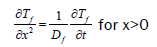
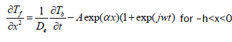
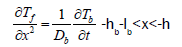
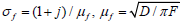 is the Thermal diffusivity and F is the modulation frequency of the heating beam. We notice that deflection is proportional to the complex temperature T0 at the sample surface. This temperature is calculated by solving the one dimension heat equation in the sample, the backing and the Surrounding fluid (Figure 3)
 (1)
(1)
 (2)
(2)
 (3)
(3)
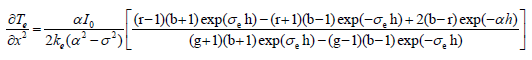
These equations are solved while taking into account of the boundary conditions at different interfaces. The obtained surface temperature is given by:
 (4)
(4)
All thermal and optical parameters that appear in the above expression are given.

Figure 3: Amplitude of the experimental photothermal signal versus square root of frequency of the samples at different anodisation currents Ia: (a) Ia=200; (b) Ia=250; (c) Ia=300; (d) Ia=400 fitted with theoretical curves (lines).
In order to determine the thermal conductivity evolutions with the anodization currents of porous alumina. We present in Figure 3a-3d the coincidence between the experimental and theoretical curves of the normalized amplitude of the photothermal signal versus the square-root modulation frequency for various porosity. These curves have the same behaviour, but we notice small difference in the slope at low and high frequencies, and also small shifts of the maximum. Thermal conductivity K of the Si incorporated in porous alumina was determined by fitting the experimental amplitude curves to the corresponding theoretical ones. We notice that the thermal conductivity decreases with the increasing of anodization currents. This behaviour comes from the presence of air inside the micropores. The sponge-like spherical or columnar morphology of micropores may also reduce the thermal transport and carrier diffusion process, clearly illustrated in Table 1.
| Anodisation currents Ia (mV) | Thermal conductivity (W.m-1.K-1 ) |
|---|---|
| 200 | 11,5 |
| 250 | 15,3 |
| 300 | 18,1 |
| 400 | 22,2 |
Table 1: Thermal conductivity of Si thin film deposited on Porous alumina at different anodisation currents
We notice a smaller thermal conductivity value (K=11.5 W. m-1. K-1) for the sample with 200 mV; it may be due to a thermal insulating effect. We remark that K decrease with anodisation currents.