


 21 / 34

Page 56
Notes:
conferenceseries
.com
RRJOMS | Volume 5 | Issue 4 | July, 2017
July 27-29, 2017 Vancouver, Canada
10
th
International Conference on
Emerging Materials and Nanotechnology
Self-organized periodic nanostructures on the surfaces of semiconductors and dielectrics by scanning
femtosecond laser pulses
Ki-Soo Lim
Chungbuk National University, Korea
W
e report the self-formed nanogratings on the surfaces of semiconductors (ZnO and GaN) and dielectric materials
(fused silica, borate glass, LiTaO
3
, LiVO
3
, sapphire) prepared by scanning focused femtosecond laser pulses at 800
nm with a repetition rate of 1 kHz. Laser fluence range for nanograting self-formation is very narrow. We found that series
of periodic-structure orientation is perpendicular to the linear laser polarization. The period of grating structures on the
dielectric surface depends on laser power and scans speed and increases in the range of 200~300 nm with scan speed and
laser pulse energy. In contrast, GaN shows about 600 nm period in the same power range as the dielectric materials. Its period
decreases to 450 nm when the laser power is reduced ten times. It also has much lower laser ablation threshold than dielectrics
and ZnO, indicating characteristics of metal-like nanogratings due to its high plasma density, large thermal conductivity, and
multiphoton absorption coefficients at 800 nm. Emission from nanograting area of sapphire indicates the existence of oxygen
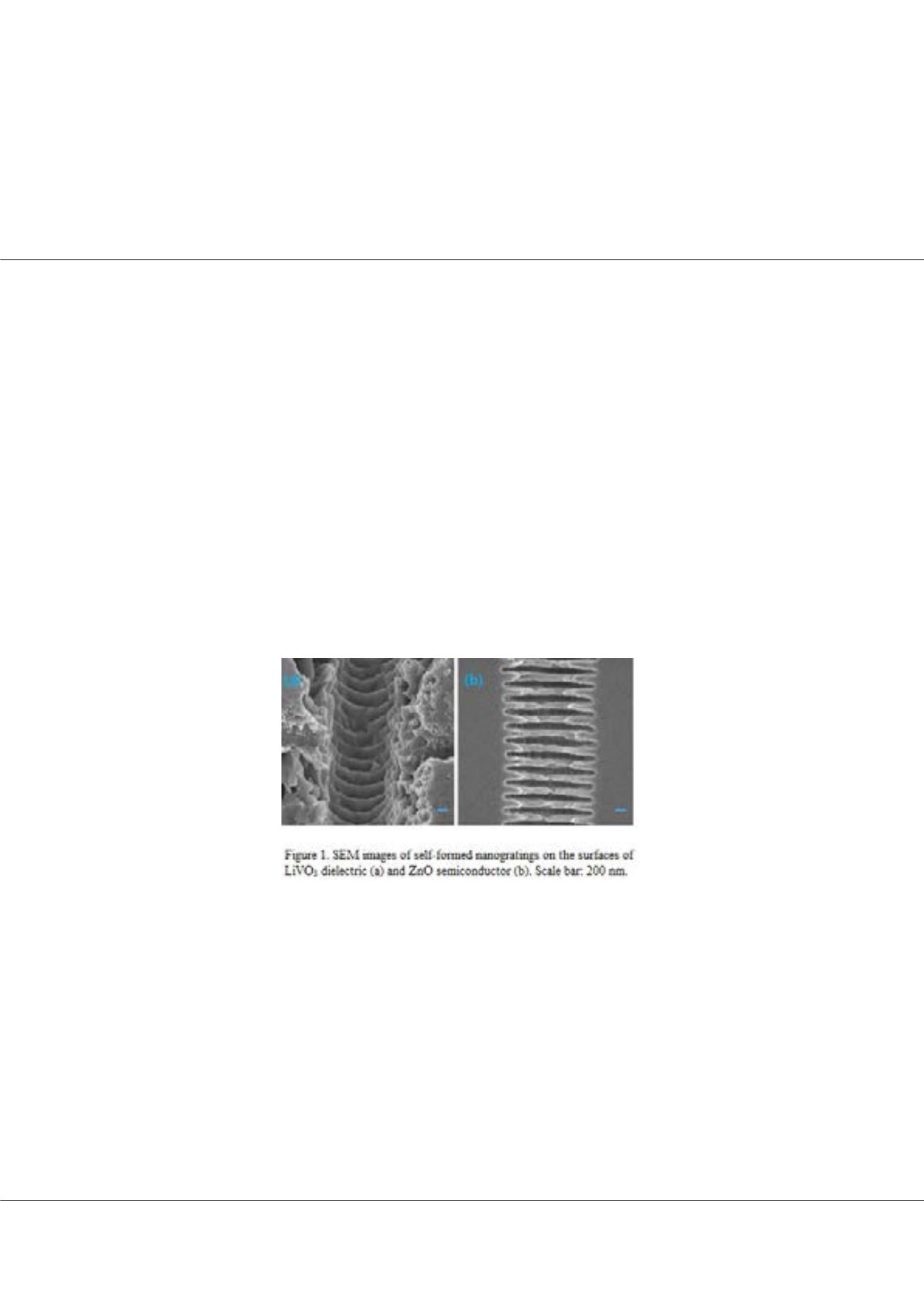
vacancies. Figure 1 shows the nanograting structure formed by scanning femtosecond laser pulses at 40 μm/s speed on the
surfaces of LiVO
3
and ZnO with 0.13 and 0.09 mW power respectively. For applications, surface nanostructures can be used
to improve out-coupling of light in LED. Material absorption can be also significantly enhanced due to surface nanostructures
produced by fs-laser pulse processing, applicable to sensing and solar cells.
Biography
Ki-Soo Lim is a Professor of Physics Department at Chungbuk National University, South Korea. He has been working on Laser Spectroscopy of rare-earth ion doped
crystals, glasses, glass-ceramics, and semiconductors. He also studied 3-D bit or holographic data storage in glass, photopolymers and photovoltaic materials.
His recent interests and achievements include precipitation and optical properties of glass-ceramics containing fluoride nanocrystals, and micro-nanostructure
fabrication on the surface of dielectric materials and polymers by femtosecond laser. He received his BS and MS degrees in Physics at Seoul National University
in 1977 and 1980 respectively. He then did his PhD in Physics at University of Connecticut, USA and worked at University of Georgia as a Research Associate. He
joined Chungbuk National University in 1990 after working at Korea Standard Research Institute..
kslim@chungbuk.ac.krKi-Soo Lim, Res. Rev. J Mat. Sci. 2017
DOI: 10.4172/2321-6212-C1-002