Keywords
|
| Clock power reduction, merging, wire length, replacement, multi-bit flip-flop. |
INTRODUCTION
|
| A clock system and a logic part consumes dominant Part of the total chip power by 20–45%. In this clock system power, 90% is consumed by the flip-flops [1]. This is due to the high switching activity. |
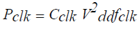 (1) (1) |
| Where Pclk is clock power, fclk is the clock frequency, Vdd is the supply voltage, and Cclk is the switching capacitance included in the gate capacitance of flip-flops. |
| During clock tree synthesis, less number of flip-flops means less number of clock sinks. Thus the resulting clock network would have smaller power consumption and uses less routing resource. The total power is reduced by replacing the 2 bit flip-flops with two 1-bit flip-flops since the two flip flops consume the same clock. However the locations of some flip-flops would be changed after this replacement and thus the wire-lengths of nets connecting pins to a flip- flop are also changed. |
| Single-bit flip-flop can be reviewed before using the multi bit flip-flop. Figure 1.1 shows an example of singlebit flip-flop. A single-bit flip-flop has two latches (Master latch and slave latch).The latches need “Clk” and “Clk’ ” signal to perform operations, shown in Figure1. |
| In order to have better delay from Clk-> Q, regenerate “Clk” from “Clk’”. Ther e ar e two inverters in the clock path. Figure 2 shows an example of merging two 1-bit flip-flops into one 2-bit flip-flop. Each 1-bit flip-flop contains two inverters, master-latch and slave-latch. Due to the manufacturing rules, inverters in flipflops tend to be oversized. |
| As the process technology advances into smaller geometry nodes, the minimum size of clock drivers can drive more than one flip-flop. Merging single-bit flip-flops into one multi-bit flip-flop can avoid duplication inverters and lowers the total clock dynamic power consumption. |
LITERATURE SURVEY
|
| 1) P. Gronowski, W. J. Bowhill, R. P. Preston, M. K. Gowan, and R.L.Allmon, “Post placement power optimization with Multi Bit Flip- Flop,” IEEE J. Solid-State Circuits, vol. 33, no. 5, pp. 676–686, May 2012. |
Concept
|
| Replacing several one bit flip flop with one Multi Bit Flip Flop to reduce the total area and dynamic power and it can be reduced upto 50%. |
Disadvantage
|
| Windows optimization technique is larger so that flip flop can perform slowly |
| 2) D. Duarte, V. Narayanan, and M. J. Irwin, “Power aware placement,” in Proc. IEEE VLSI Comput. Soc. Annu. Symp.,Pittsburgh, PA, Apr. 2005, pp. 52–57. |
Concept
|
| Focuses on calculating the idle period of different flip flop and inserting the gating logic into netlist to achieve the total power by 25.3%. |
Disadvantages
|
| The net switching power can be achieved by 25.4 % and then wirelength can also be reduced. |
| 3) H. Kawagachi and T. Sakurai, “Impact of technology scaling in the clock power,” in VLSI Circuits Dig. Tech. Papers Symp., Jun. 2003, pp. 97–98. |
Concept
|
| Increase the flexibility that covers the clock distribution and clock generation circuit to consume total power by 40%. |
Disadvantage
|
| Clock skew problem can be reduced by 30%. |
| 4)W. Hou, D. Liu, and P.-H. Ho, “Automatic register banking for low power clock trees,” in Proc. Quality Electron. Design, San Jose, Mar. 2010, pp. 647–652 |
Concept
|
| Replacing some flip flop with multibit flip flop without affecting the performance and total wire length can be minimized by 20-30%. |
Disadvantage
|
| Using dual bit flip flop to save the clock power in 11 .22% and the replacement of flip flop during switching rate is 10.43%. |
| 5) Y. Cheon, P.-H. Ho, A. B. Kahng, S. Reda, and Q. Wang, “High performance microprocessor design,” in Proc. Design Autom. Conf., Jun. `1998, pp. 795–800. |
Concept
|
| Focuss on high frequency design to achieve high performance and to improve the complexity of the circuit. |
Disadvantage
|
| In single supply voltage system reduce the clock power 25.45 %, and in multiple supply voltage system the clock power can be reduced by 26.15 %. |
PROPOSED ALGORITHM
|
| T h e Design flow can be roughly divided into three stages. First to use the combination table to combine all possible combinations of flip-flops. The difficulty of this problem is to repeatedly search a set of flip-flops that can be replaced by a new multi-bit flip-flop. However as the number of flip-flops in a chip increases dramatically the complexity would increase exponentially which makes the method impractical. To handle this problem more efficiently and to get better results, the following flowchart were used. The figure 3 shows the various approaches used in the algorithm. |
| 1) To facilitate the identification of mergeable flip- flops transform the coordinate system of cells. In this way the memory used to record the feasible placement region can also be reduced. |
| 2) To avoid wasting time in finding impossible combinations of flip-flops, first build a combination table before actually merging two flip-flops. For example, if a library only provides three kinds of flip-flops which are 1-, 2-, and 3-bit first to separate the flip-flops into three groups. Therefore the combination of 1- and 3-bit flip-flops is not considered since the library does not provide the type of 4-bit flip-flop. |
| 3) Partition a chip into several sub regions and perform replacement in each sub region to reduce the complexity. However, this method may degrade the solutions quality. To resolve the problem use a hierarchical way to enhance the result |
A. Region partition to identify the mergeable flip-flop
|
| To reduce the complexity, first divide the whole placement region into several sub-regions and then by using the combination table replace the flip-flops in each other sub- region. Then several sub-regions are combined into a larger sub-region and the flip-flops are replaced again so that those flip-flops in the neighboring sub-regions can be replaced further. Finally those flip-flops with pseudo types are deleted in the last stage as it is not provided by the supported library. |
B. Replacement of flip-flop
|
| After a combination has been built do the replacements of flip-flops according to the combination table. First flipflops below the combinations corresponding to their types in the library were linked. Then for each combination n in T, serially merge the flip-flops linked below the left child and the right child of n from leaves to root. Based on its binary tree to find the combinations associated with the left child and right child of the root. Hence the flip-flops in the lists named left and lright, linked below the combinations of its left child and its right child are checked. Then for each flip-flop f i in lleft the best flip-flop fbest in lright which is the flip-flop that can be merged with f i with the smallest cost recorded in cbest, is picked. For each pair of flip-flops the combination cost is computed and they can be merged with the smallest cost as chosen. Finally add a new flip-flop f in the list of the combination n and remove the picked flip-flops which constitutes the f .For example, given a library containing three types of flip-flops (1-, 2-, and 4- bit), first to build a combination table T as shown in Figure5. |
| The above figure says that |
| (a) Sets of flip-flops before merging. |
| (b) Two 1-bit flip-flops, f1 and f2, are replaced by the 2-bit flip-flop f3. |
| (c) Two 1-bit flip-flops, f4 and f5, are replaced by the 2-bit flip-flop f6. |
| (d) Two 2-bit flip-flops, f7 and f8, are replaced by the 4-bit flip-flop f9. |
| (e) Two 2-bit flip-flops, f3 and f6, are replaced by the 4-bit flip-flop f10. |
| (f) Sets of flip-flops after merging. |
| In the beginning, the flip-flops with various types are, respectively, linked below n1, n2, and n3 in T according to their types. Suppose to form a flip-flop in n4 which needs two 1-bit flip-flops according to the combination table then each pair of flip-flops in n1 are selected and checked to see if they can be combined .If there are several possible choices the pair with the smallest cost value is chosen to break the tie. |
C. Combination table and merging flip-flop
|
| Finally add a new flip-flop f in the list of the combination n and remove the picked flip-flops which constitutes the f .Pseudo type is an intermediate type which is used to enumerate all possible combinations in the combination table T, then to remove the flip-flops belonging to pseudo types. Thus after the above procedures have been applied de-replacement and replacement functions are performed if there exists any flop-flops belonging to a pseudo type is shown in figure 6. |
| The figure says that |
| (a) Initialize the library Land the combination table T . |
| (b) Pseudo types are added into L, and the corresponding binary tree is also build. |
| (c) New combination n3 is obtained from combining two n1s. (d) New combination n4 is obtained from combining n1 and n3. |
| (e) New combination n6 is obtained from combiningn1 and n4. (f) Last combination table is obtained after deleting unused combination in (e). |
| For example, if there still exists a flip-flop, fi , belonging to n3 after replacements in Fig (Fig. Last combination table is obtained after deleting the unused combination), then to de-replace fi into two flip-flops originally belongs to n1. After de-replacing, the replacements of flip-flops according to T without consideration of the combinations whose corresponding type is pseudo in L were built. |
COMPARISON TABLE FOR VARIOUS METHODS
|
| This table specifies the various implementation of flip-flop to optimize the power and to achieve the net switching activity. Although the drivers are very wide devices it was found that for all technologies the share of the clock power that is due to leakage is at most 2.5%. Technology optimizations and dynamic runtime techniques forleakage reduction wi l l become standard for clock power and will remain a major contributor to the total system power. |
CONVENTIONAL CONDITIONAL DATA MAPPING
|
D FLIP-FLOP
|
| In conditional data mapping flip-flop (CDMFF) uses only s e v e n clocked transistors, r e s u l t i n g in about 50% reductions in the number of clocked transistors. This shows the effectiveness of reducing clocked transistor numbers to achieve low power. The figure 7 shows the circuit diagram for CDMFF. |
| In a Conventional D flip-flop part of the clock energy is consumed by the internal clock buffer to control the transmission gates. |
CLOCKED PAIR SHARED FLIP-FLOP DESIGN
|
| To ensure efficient and robust implementation of low power sequential element propose a Clocked Pair Shared flip-flop to use less clocked transistor than CDMFF and to overcome the floating problem in CDMFF.The figure 8 shows the block diagram of CPSFF. |
| By reducing the no of transistor count the overall switching delay, power, and area consumption can be reduced. LOW POWER CLOCKED PASS TRANSISTOR FLIP- FLOP Low Power Clocked Pass Transistor flip-flop design shows much less power & Area constraints than the Existing two Flip-Flop designs. LCPTFF will be having very less clock delay when compared to all other circuits. |
OUTPUT WAVEFORM
|
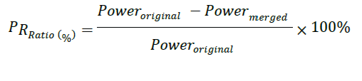
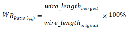
| The values PR_Ratio and WR_Ratio can be computed by the following equations |
 |
 |
CONCLUSION
|
| The number of flip-flops in a chip increases dramatically the complexity would increase exponentially, which makes the method impractical. To handle this problem more efficiently and get better results, the following approaches are used.1) To facilitate the identification of mergeable flip-flops transform the coordinate system of cells. In this way the memory used to record the feasible placement region can also be reduced.2) To avoid wasting time in finding impossible combinations of flip-flops first build a combination table before actually merging two lipflops. 3) Partition a chip into several sub-regions and perform replacement in each sub-region to reduce the complexity. However this method may degrade the solution quality. To resolve the problem use a hierarchical way to enhance the result and processing time can be reduced. |
Tables at a glance
|
|
|
| |
Figures at a glance
|
 |
 |
 |
 |
 |
| Figure 1 |
Figure 2 |
Figure 3 |
Figure 4 |
Figure 5 |
| |
 |
 |
 |
 |
 |
| Figure 6 |
Figure 7 |
Figure 8 |
Figure 9 |
Figure 10 |
| |
 |
 |
 |
| Figure 11 |
Figure 12 |
Figure 13 |
|
| |
References
|
- Y.-T. Chang, C.-C.Hsu, P.-H.Lin, Y.-W.Tsai, and S.-F. Chen,“Post-placement power optimization with multi-bit flip- flops,” in Proc.IEEE/ACMComputer.-Aided Design Int. Conf., San Jose, CA, ,pp. 218–223, Nov. 2010.
- D. Duarte, V. Narayanan, and M. J. Irwin, “Impact of technology scaling in the clock power,” In Proc. IEEE VLSI Comput. Soc. Annu. Symp.,Pittsburgh, PA, , pp. 52–57, Apr. 2002.
- Y. Cheon, P.-H. Ho, A. B. Kahng, S. Reda, and Q. Wang,“Power-aware placement,” in Proc. Design Autom. Conf, pp. 795–800 Jun.2005.
- Yu-Cheng Lin, Guo-SyuanLiou,Tsai-Ming Hsieh,“Using Multi-Bit Flip-Flop For Clock Power Saving By Designcompiler”, July-12/2006
- Y. J. Yu and Y. C. Lim, “Impact of scaling on the effectiveness of dynamic power reduction schemes,” IEEE Trans. CircuitsSyst. I, Reg.Papers, vol. 54, no. 10, pp. 2330–2338, Oct. 2002.
- D. Shi and Y. J. Yu, “A new reduced clock power flip flop for future Soc’s application,” IEEE Trans. Circuits Syst.I, Reg. Papers, vol. 58, no.1,pp. 126–136, Jan. 2012.
- H.A Chien, C.C Lin, H.H Huang, T.M Hsieh, “ Clock network power saving using Multi Bit Flip-Flop in Multiple voltage Design,”IEICETRANSACTIONS on Fundamentals of Electronics, Communications and Computer Sciences, pp.761-768, 2010.
- C. Bron and J. Kerbosch, “Algorithm 457: Finding all cliques of and undirected graph,” ACM Commun., vol. 16, no.9, pp. 575–577, 1973.
- L. Huang, Y. Cai, Q. Zhou, X. Hong, J. Hu, and Y. Lu, “Clock network minimization methodology based on incremental placement,” in Proc.IEEE/ACM Asia South Pacific Des. Autom. Conf., Jan. 2005,pp. 99–102.
|