Keywords
|
| single-path delay feedback, bit-parallel multipliers, low power. |
INTRODUCTION
|
| Due to the popularity of the communication systems, the Fourier transform is still one of research and development topics in the radio transmission and mobile communication. However, for the operation of discrete Fourier transform in real-time signal processing system, it is important to get the operation results in time. Therefore, fast Fourier transform (FFT) is the suitable choice for this purpose since the computational complexity is reduced from O(N2)to O(N log N) . The high-speed performance and hardware reduction can be attained. |
| The main trends of FFT hardware development are towards high throughput and low power consumption. The pipelined structure is the most common choice for high-throughput FFT processor. Many methods have been proposed to implement the pipelined FFT hardware architectures. They can be categorized into three kinds, namely, the multiple-path delay commutator (MDC), single-path delay feedback (SDF), and single-path delay commutator (SDC) architectures. In comparison with the three pipeline architectures, the SDF architecture is the most suitable for FFT implementation. Its advantages are (i).the SDF architecture is very simple to implement the different length FFT, (ii).the required registers in SDF architecture is less than MDC and SDC architectures,(iii).The control unit of SDF architecture is easier than the others. |
A. DISCRETE FOURIER TRANSFORM
|
| Discrete Fourier transform (DFT) is a very important technique in modern digital signal processing (DSP) and telecommunications, especially for applications in orthogonal frequency demodulation multiplexing (OFDM) systems, such as IEEE 802.11a/g , Worldwide Interoperability for Microwave Access (WiMAX) , Long Term Evolution(LTE), and Digital Video Broadcasting—Terrestrial(DVB-T) . However, DFT is computational intensive and has a time complexity of O(N2). The fast Fourier Transform (FFT) was proposed by Cooley and Tukey to efficiently reduce the time complexity to O (N log 2N), where N denotes the FFT size. |
| For hardware implementation, various FFT processors have been proposed. These implementations can be mainly classified into memory-based and pipeline architecture styles. Memory-based architecture is widely adopted to design an FFT processor, also known as the single processing element (PE) approach. This design style is usually composed of a main PE and several memory units, thus the hardware cost and the power consumption are both lower than the other architecture style. However, this kind of architecture style has long latency, low throughput, and cannot be parallelized. On the other hand, the pipeline architecture style can get rid off the disadvantages of the foregoing style, at the cost of an acceptable hardware overhead. The single-path delay feedback (SDF) pipeline FFT is good in its requiring less memory space (about N-1 delay elements) and its multiplication computation utilization being less than 50%, as well as its control unit being easy to design. Such implementations are advantageous to low-power design, especially for applications in portable DSP devices. Based on these reasons, the SDF pipeline FFT is adopted in this work. However, the FFT computation often needs to multiply input signals with different twiddle factors for an outcome, which results in higher hardware cost because a large size of ROM is needed to store the wanted twiddle factors. Therefore, to throw off these ROM’s for area-efficient consideration. |
B.COMPLEX MULTIPLIERS
|
| The complex multipliers used in the processor are realized with shift-and-add operations. Hence, the processor uses only a two-input digital multiplier and does not need any ROM for internal storage of coefficients. However, low speed and higher hardware cost caused by the proposed complex multiplier are the pay-off. In order to further improve the power consumption and chip area of previous works, this paper proposes an efficient radix-2 pipeline architecture with low power consumption for the FFT/IFFT processor. The proposed architecture includes a reconfigurable complex constant multiplier and bit-parallel complex multipliers instead of using ROM’s to store twiddle factors, which is suited for the power-of-2 radix style of FFT/IFFT processors. |
METHODOLOGY
|
A. ORTHOGONAL FREQUENCY DIVISION MULTIPLEXING
|
| OFDM is the abbreviation for Orthogonal Frequency Division Multiplexing, and describes a digital modulation scheme that distributes a single data stream over a large number of carriers for parallel transmission. These carriers are called the subcarriers of the signal. In the frequency domain, they are equally spaced around a central RF carrier, so the frequency fn,rf of the nth subcarrier out of N can be expressed as |
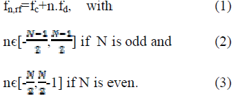 |
| fd is the frequency spacing between the subcarriers and fc is the center frequency of the OFDM signal. |
| In the baseband, we obtain |
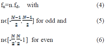 |
| where fn is the baseband frequency of the nth subcarrier. |
| The subcarriers exp(2*Pi*n*fd*t) build an orthogonal set of functions, hence the name of the modulation. Each of these subcarriers is modulated separately. The modulation symbols result from encoding the binary data using traditional PSK or QAM mappings. Let us assume we want to transmit 128 bits simultaneously on N = 64 QPSK modulated subcarriers (n = -32, -31..., +31). Then for example the subcarrier with index -32 may carry the first pair of bits, the subcarrier with index -31 would carry thesecond pair, and so on. The last two bits would then be assigned to the subcarrier with index +31. |
| So, within one OFDM symbol, each subcarrier has its own phase pn and amplitude an. The whole baseband signal looks like this: |
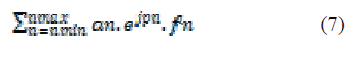 |
| Where nmin and nmax set the range for n. |
| We can interpret this as the Discrete Fourier Transform (DFT) of the OFDM symbol to generate. Consequently, instead of really modulatingall 64 subcarriers, the discrete time domain signal is calculated by applying to s an inverse DFT of length N. The result is a series of samples that represent one period of a signal that has the same spectrum as the desired OFDM symbol. The sampling frequency is fs = N*fd. One period of the calculated series yields all amplitude and phase information contained in s. The minimum OFDM Symbol duration is thus |
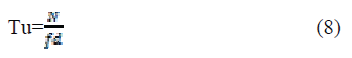 |
| If N is chosen to be power of 2, an inverse fast Fourier transform (FFT) can be used instead of the more time consuming DFT. Notice that the DFT is defined for signals that are periodic in the time domain aswell as in the frequency domain. The alias spectra are eliminated through (digital) baseband filtering. Therefore, it is necessary to leave some empty space at the high and low end of the DFT spectrum s forthe filter to cut in. Thus, only a subset of the N maximum possible subcarriers will actually be modulated, the others have zero amplitude. |
| B. TWIDDLE FACTOR |
| A twiddle factor, in fast Fourier transform (FFT) algorithms, is any of the trigonometric constant coefficients that are multiplied by the data in the course of the algorithm "twiddle factors" originally referred to the root-ofunity complex multiplicative constants in the butterfly operations of the Cooley-Tukey FFT algorithm, used to recursively combine smaller discrete Fourier transforms. This remains the term's most common meaning, but it may also be used for any data-independent multiplicative constant in an FFT. |
| The Prime-factor FFT algorithm is one unusual case in which an FFT can be performed without twiddle factors, only for restricted factorizations of the transform size. |
C. DISCRETE FOURIER TRANSFORM
|
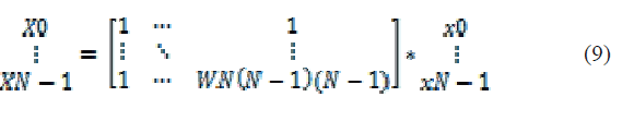 |
| {Xk} is periodic |
| Since {Xk} is sampled, {xn} must also be periodic |
| From a physical point of view, both are repeated with period N and requires O(N2) operations. |
D. THE COST OF MAPPING
|
| Different types balance mapping with sub problem cost |
| (i) in radix-2 |
| • Sub problems are trivial (only sum and differences) |
| • Mapping requires twiddle factors (large number of multiplies) |
| (ii)in prime-factor algorithm |
| • Sub problems are DFTs with co-prime lengths (costly) |
| • Mapping trivial (no arithmetic operations) |
E.FFT PROCESSOR MEMORY-SYSTEM ARCHITECTURES
|
| As with most DSP algorithms, FFT’s make frequent accesses to data in memory. FFT’s are calculated in O(log N) stages, where N is the length of the transform and is the radix of the FFT decomposition. Each stage requires the reading and writing of all N data words. |
| 1) Single Memory: The simplest memory-system architecture is the single-memory architecture, as shown in Fig. 1,in which a memory of at least N words is connected to a processor by a bidirectional data bus. In general, data are read from and written back to the memory once for each of the log N stages of the FFT. |
| 2) Dual Memory: The dual-memory architecture places two memories of size N on separate buses connected to a processor, as Fig. 2 shows. Data begin in one memory and “ping-pong” from memory to memory log N times until the transform has been calculated. The Honeywell DASP processor and the Sharp LH9124 processor use the dual-memory architecture. |
| 3) Pipeline: For processors using a pipeline architecture, a series of smaller memories replace the -word memory(ies).Either physically or logically, there are log N stages. Fig. 3shows how processors and buffer memories are interleaved as well as the flow of data through the pipeline structure. Typically, an -word memory is on one end of the pipeline, and memory sizes increase by through subsequent stages, with the final memory of size . The Logic Corp. (LSI) L64280 FFT processor, the FFT processor designed by Heand Torkelson, and the FFT processor by Bidet et al. use pipeline architectures. |
| 4) Array: Processors using an array architecture are composed of a number of independent processing elements with local buffers, interconnected through some type of network, as depicted in Fig. 4. The Cobra FFT processor uses an array architecture and is composed of multiple chips that each contains one processor and one local buffer. The FFT processor by O’Brien et al. uses an array-style architecture with four data paths and four memory banks on a single chip. |
EXISTING SYSTEM
|
| The canonic signed digit (CSD) representation is used to design the function of complex multiplier, which is the main function block in the FFT processor. The processor of a 16-bit 16-point pipeline FFT is realized on the Xilinx Virtex- 4 FPGAs. The achieved maximum clock frequency is 196.8 MHz, utilizing 310 out of 49152 slices and 241 out of 98304 look-up tables. Another 16-bit 64-point pipeline FFT processor is also realized. The achieved maximum clock frequency is 111.2 MHz, utilizing 1303 out of 49152 slices and 2065 out of 98304 look-up tables. Comparing with the conventional complex multiplier, the derived results show the proposed design has improved efficiency on Virtex-4. |
| The main trends of FFT hardware development are toward high throughput and low power consumption. The pipelined structure is the most common choice for high-throughput FFT processor. The word lengths of various signals are minimized according to their respective signal-to-noise ratio(SNR) requirements. To decide the optimal word length, input waveforms with Gaussian noise are fed to the FFT with fixed-point arithmetic implementation. The frequency domain FFT output signals are obtained and the output signal-to-noise ratio (SNR) is computed. The CORDIC algorithm has been used for the twiddle factor multiplication in FFT processors due to its efficiency invector rotation. In this sub-Section, we evaluate and compare the performance and complexity of a CORDIC and a complex multiplier in phase rotation. The conventional CORDIC algorithm refers to the radix-2CORDIC, and radix-2=4 CORDIC refers to the work in that enhances operation speed and reduces 25% of the micro-rotation stages. The complex multiplier used in the proposed chip consists of three multiplications and five additions .To make a fair comparison, we set the precision to 16 bits in all algorithms. To avoid rounding error propagation, 19 bits are allocated in the data path of the CORDIC-based architectures. |
A. MODIFIED COMPLEX MULTIPLIER
|
| The conventional complex multiplication this architecture needs four multipliers and two adders. (x+xi) (y+yi)=(x.y+xi.yi) (xi.y+x.yi) |
| Conventional complex multiplier structure for the pipeline FFT processors, their performances depend on the arithmetic operation of the complex multipliers. To increase the overall operational speed, reduce area and power consumption, an efficient implementation of complex multipliers is very important. The canonic signed digit (CSD) representation is chosen for realizing complex multipliers because it yields significant hardware reduction comparing with conventional complex multiplier .The CSD unit consists of many shifters and adders. It is used to realize the multiplication when the one factor is constant. The CSD unit is used to construct a complex multiplier. Since CSD representation of a number contains the minimum possible number of non-zero bits for the range (-4/3, 4/3), the CSD blocks for the complex computing of multiplication in Fig. 2 need fewer adders and hence the power consumption and area can be reduced by about 33% |
B.HARDWARE REALIZATION
|
| The design of a 16-point pipeline radix-2 SDF FFT is implemented on the Xilinx Virtex-4 xc4vlx100. The achieved maximum clock frequency is 196.8MHz. It utilizes 310 out of49152 slices and 241 out of 98304 look-up tables. The 64-pointpipeline radix-22 SDF FFT is also realized on the XilinxVirtex-4 xc4vlx100. It achieves the maximum clock frequency of 111.182MHz and utilizes 1303 out of 49152 slices, 2065 out of 98304 look-up tables. Due to the efficiency of Booth multiplier, it is wide applied to realize the conventional complex multiplier. Comparing the realized complex multipliers on the Xilinx FPGA of [10] with our complex multiplier, improved performances of the presented complex multiplier can be obtained. The efficiency of the circuit is quantified by throughput per unit of area (MHz /CLB). The comparison is shown in table. |
PROPOSED SYSTEM
|
| Memory-based architecture is widely adopted to design an FFT processor, also known as the single processing element (PE) approach. This deign style is usually composed of a main PE and several memory units, thus the hardware cost and the power consumption are both lower than the other architecture style. However, this kind of architecture style has long latency, low throughput, and cannot be parallelized. On the other hand, the pipeline architecture style can get ridoff the disadvantages of the foregoing style, at the cost of an acceptable hardware overhead. |
| In order to improve the previous works on power reduction, we propose a radix-2 64-point pipeline FFT/IFFT processor with low power consumption. The proposed architecture is composed of three different types of processing elements (PEs), a complex constant multiplier, delay-line (DL) buffers (as shown by a rectangle with a number inside), and some extra processing units for computing IFFT. Here, the conjugate for extra processing units is easy to implement, which only takes the 2’scomplement of the imaginary part of a complex value. Thedivided-by-64 module can be substituted with a barrel shifter. |
| In addition, for a complex constant multiplier, here it is proposed a novel reconfigurable complex constant multiplier to eliminate the twiddle-factor ROM. This new multiplication structure thus becomes the key component in reducing the chip area and power consumption of our proposed FFT/IFFT processor. |
A. PROCESSING ELEMENTS
|
| Based on the radix-2 FFT algorithm, three types of processing elements (PE3, PE2, and PE1) used. The functions of these three PE types correspond to each of the butterfly. First, the PE3 stage is used to implement a simple radix-2 butterfly structure only, and serves as the sub-modules of the PE2 and PE1 stages. In the figure, Iin and Iout are the real parts of the input and output data, respectively. Qin and Qout denote the image parts of the input and output data, respectively. Similarly, DL_Iin and DL_Iout stand for the real parts of input and output of the DL buffers, and DL_Qin and DL_Qout are for the image parts, respectively. |
| As for the PE2 stage, it is required to compute the multiplication by –j or 1. Note that the multiplication by -1 is practically to take the 2’s complement of its input value. In the PE1 stage, the calculation is more complex than thePE2 stage, which is responsible for computing the multiplications by –j, WN N/8 and WN 3N/8 respectively Since WN 3N/8 ==-j WN N/8 it can be given by either the multiplication by WN N/k first and then the multiplication by –j or the reverse of the previous calculation. Hence, the designed hardware utilizes this kind of cascaded calculation and multiplexers to realize all the necessary calculations of the PE1 stage. This manner can also save a bit-parallel multiplier for computing WN N/k which further forms a low-cost hardware. |
B. BIT-PARALLEL MULTIPLIERS
|
| The multiplication by 1/√ 2 can employ a bit-parallel multiplier to replace the word length multiplier and square root evaluation for chip area reduction. The bit-parallel operation in terms of power of 2 is given by, |
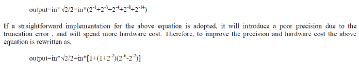 |
| The circuit diagram of the bit-parallel multiplier is illustrated in Fig. 7. The resulting circuit uses three additions and three barrel shift operations. The realization of complex multiplication by WN N/8 using a radix-2 butterfly structure with its both outputs commonly multiplied by 1/ √2 is shown in Fig. 8. This circuit has just been used in the PE1 stage. |
C. RECONFIGURABLE COMPLEX CONSTANT MULTIPLIERS
|
| A reconfigurable low-complexity complex constant multiplier for computing W i64 is proposed, as shown in Fig.9.This structure of this complex multiplier also adopts a cascaded scheme to achieve low-cost hardware. Here, the meaning of two input signals (Iin and Iout)and two output signals (Qin and Qout) are the same as the signals in the PE1 stage. |
| This circuit is responsible for the computation of multiplication by a twiddle factor W i64, which is also an important circuit of our FFT/IFFT processor. The word-length multiplier used adopts a low-error fixed width modified Booth multiplier for hardware cost reduction. The coefficient values i1-i8 and q1-q8 are listed in Table 2,which can be used to synthesize the entire twiddle factors required in our proposed 64-point FFT processor. |
CONCLUSION
|
| A novel ROM-less and low-power pipeline 64-point FFT/IFFT processor for OFDM applications has been described in this paper. We have designed a reconfigurable complex constant multiplier such that the size of twiddle-factor ROM is significantly shrunk, especially no ROM is needed. This result shows that this design owns lower hardware cost and power consumption compared to the existing ones. Of course, our proposed scheme can also be adapted to high-point FFT applications, with a lower size oft widdle-factor ROM’s. It can serve as a powerful FFT/IFFT processor in many other wireless communication systems. |
Tables at a glance
|
 |
|
| Table 1 |
Table 2 |
|
Figures at a glance
|
 |
 |
 |
 |
 |
| Figure 1 |
Figure 2 |
Figure 3 |
Figure 4 |
Figure 5 |
 |
 |
 |
 |
| Figure 6 |
Figure 7 |
Figure 8 |
Figure 9 |
|
References
|
- IEEE Std 802.11a, 1999, “Wireless LAN Medium Access Control (MAC) and Physical Layer (PHY) specifications: High-Speed Physical Layer in the 5 GHz band.”
- IEEE 802.16, IEEE Standard for Air Interface for Fixed Broadband Wireless Access Systems, the Institute of Electrical and Electronics Engineers, Inc., June 2004.
- GPP LTE, “Evolved Universal Terrestrial Radio Access (E-UTRA); Physical Channels and Modulation” 3GPP TS 36.211 v8.5.0, 2008-12.
- ETSI, “Digital Video Broadcasting (DVB); Framing Structure, Channel Coding and Modulation for Digital Terrestrial Television,” ETSI EN 300 744 v1.4.1, 2001.
- J. W. Cooley and J. W. Tukey, “An algorithm for the machine calculation of complex Fourier series,” Math. Comput., vol. 19, pp. 297- 301, Apr. 1965
- Minhyeok Shin and Hanho Lee, “A High-Speed Four-Parallel Radix-24 FFT/IFFT Processor for UWB Applications,” in Proc. IEEE Int. Symp. Circuits and Systems, 2008, pp. 960-963
- Wen-Chang Yeh and Chein-Wei Jen, “High-speed and low-power splitradix FFT,” IEEE Transactions on SignalProcessing, vol. 51, no. 3, pp. 864- 874, Mar. 2003.
|