Keywords
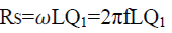
|
| Concurrency, Dual Band Filter, Dual Band Amplifier, Dual Detection, Frequency Multiplier |
INTRODUCTION
|
| The common radio transmission and reception activities are accomplished through modulation at single carrier frequency. When the communication channel vary by the presence of dust particles, raindrops or snows the scattering and diffracting abilities of these tiny masses, cause detrimental effects to the smooth propagation of these radio carrier waves and thus spoil the communication activities. |
| Solution to this effect could be achieved, by increasing the signal strength of the radio signal or by changing the carrier frequency which has direct link to these effects, since they are wavelength dependent. The latter solution is more economical and technically feasible. It was suggested by Wu,S and Razavi,B, Fong, k and Ryynanen,J. |
| In this work, we wish to present an architecture that would provide concurrency in the dual transmission and reception of the modulated carrier above, with additional modification of the previous works on the detection section. |
| Most of today’s wireless receivers use any of these general architectures: heterodyne, homodyne, low-IF, and imagerejection receivers such as the ones originally proposed by D. K. Weaver. Similarly, all these architectures have been employed in the multi-band receivers for various applications. |
| Direct conversion receiver represents a less complicated design by having a reduced number of circuit blocks, number of stages; provide a wide tuning range and high selectivity. There is however several drawbacks such as two high frequency conversion stages in parallel, local oscillator signal may cause leakage to the antenna. The reduce circuit complexity generally reduced performance; problem of image in this architecture is form when the size of noise or any interference is closed to or above the size of signal. |
| That problem of image with direct conversion can be overcome using superheterodyne receiver. This is the traditional radio receiver architecture for wireless communication. The solution is to place a filter before the mixer to remove the image. A very high quality band pass filter is needed, to provide the desired performance. To achieve good selectivity by down-converting the received RF signal in multiple steps. In multi-band heterodyne radio architecture, there will be higher power consumption, and a higher overall cost for the system, translation. Also at the end, the received signal information, though of high quality, is usually weak. |
| To solve the problem of weak signal in super heterodyne architecture,[18] suggested parallel dual detection. When the final output is added, the signal is obtained. This architecture increases the signal strange. The weaver solution is restricted to the signal already received by the radio. If the signal suffered in the channel before reaching the receiver, the weaver solution is ineffective.[17] proposed a modification in which the transmission and reception are going to be done at two different frequencies. |
| The problem of power consumption of the above architecture was considered by [6], and led them to a circuit with a dual band low noise amplifier using single wide band amplifier and dual band filter for the two carrier frequencies. However this architecture needs two local oscillators for detection of f1 and f2. |
| In this work we proposed the use of a single LO with a frequency multiplier instead of double oscillators in the Hossein. H and Hajimiri,A. |
CONCURRENT DUAL BAND RADIO RECEIVER
|
| In the [6], two distinct oscillators were used. In this work, we intend to use a single oscillator with a doubler circuit during detection. This may reduce the cost of the final circuit. The proposed architecture is illustrated in figure 1. |
| The circuit block includes an antenna, which received modulated signals of the same information at different frequencies. The modulated signals passed through a dual band-band pass filter (BPF), to select the desired frequencies f1 and f2 and reject or block the undesired ones. These signals are then amplified by a very wideband amplifier with turning at f1 and f2 concurrently. The last stage is dual detection, where modulated frequency f1 is mixed with carrier frequency FC1 of LO to produce intermediate frequency (If1). Also the signal f1 from the LO is doubled in the multiplier, and mixed with modulated frequency f2 to produce intermediate frequency (If2). The designs of these three circuits; the dual band filter, the amplifier and the frequency multiplier are presented below. |
FILTER DESIGN
|
| The design architecture of the filter used in this work was the one proposed by [13] .and follow chebyshev configuration. It is simple and has the advantage of using identical conductor throughout the filter sections beside its excellent design flexibility and high performance. |
| For dual band filters, the architecture proposed by [12] and [1] modified by [11] is used in which the architecture dual band filter is achieved by inserting a narrow band top filter into a broadband filter to create the dual band characteristics. It is presented in fig 2. |
| The figure above shows three stages of two single band filters, to select f1 and f2 connected in parallel, with input from the left and output at the right side of the circuit. |
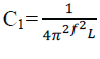
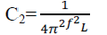
| To design such filter, it requires Center frequency (f0), bandwidth (BW), pass-band ripple (rp), input and output impedances (Zi and Zo), number of stages (ns) and the shunt inductor value (L) to be used. Using these parameters, the capacitance and Q factor values were computed. |
| Center Frequency,(900MHz and 1800MHz) Bandwidth (Hz) BW=25MHz (G.S.M Band)Pass band Ripple = 1 dB [16] Inductance, L=0.1nH |
 (1) (1) |
 |
DUAL BAND FILTER DESIGN
|
| Recent researches on the design of dual-band BPFs have been presented [1]. One of simplest methods to design the dual-band BPF is by connecting two different pass band BPFs in parallel to obtain the dual-band characteristics. Another approach is to insert a narrowband band stop filter into the broadband BPF to create the dual-band characteristics.[11].Because two different filters are used, the sizes of these dual-band BPF are comparatively large. |
 |
| The output and input impedance to be connected in series is given with |
| Rp=211.6Ω Impedance Z=50Ω |
| Therefore single band BPF of f1&f2 designed above can form a dual band BPF with two signals by connecting the two single bands in parallel. The fig. 3 above shows the circuit diagram of dual band BPF. |
DUAL BAND AMPLIFIER
|
| In conventional dual-band amplifier, either one of the two single-band amplifier is selected [14][5], or two singleband amplifier are designed to work in parallel using two separate resonant loads, resulting in a high implementation cost due to the large chip area [17]. The former approach is non-concurrent, while the latter consumes twice as much power. In a wideband LNA, strong unwanted blockers are amplified together with the desired frequency bands and significantly degrade the receiver sensitivity. In this work, concurrent multiband amplifier was proposed as an alternative to alleviate these problems, using bipolar junction transistor (BJT) for wide band operation. |
| Dual band amplifier is achieved by using a wave band amplifier and tuning within its pass band, the two desired frequencies f1 and f2. |
AMPLIFIER DESIGN
|
| The figure above shows main function of concurrency. An amplifier built around transistor, NPN RF Input Power of SiGe:C Bipolar Transistor BFR740L3RH, with Common source configuration. Contains input and output impedances, series resonance circuit and parallel resonance at the output, which turn to amplify f1 and f2 at the output |
| The circuit design starts with data sheet. [10] silicon configurations were used |
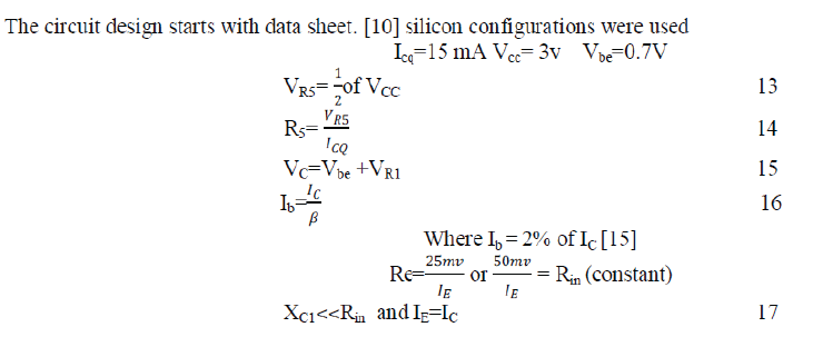 |
| The capacitor is chosen with reference to the lower frequency f1 with impedance so that any frequency above f1 with lower impedance will be amplified. |
SERIES RESONANCE CIRCUIT
|
| To excite a crystal for operation in series resonant mode, it may be connected as a series element in feedback path. At the series resonant frequency of the crystal, its impedance is smallest and the amount of positive feedback is largest. At series resonant frequency f1, inductor l1=10nH (assumed) |
 (18) (18) |
PARALLEL RESONANCE CIRCUIT
|
| Since the parallel resonant impedance of a crystal is a maximum in shunt. At the parallel resonance operating frequency, a crystal appears as an inductive reactance of largest value. |
| At parallel resonant frequency f2, inductor L1=10nH |
 (19) (19) |
| The output impedance must be far greater than the input impedance of the next stage, assume Z=50Ω |
 (20) (20) |
AMPLIFIER DESIGN ANALYSIS
|
| This aspect expressed the general amplifier analysis to transfer function of an amplifier gain. The equivalent model of the circuit is given in the figure below; |
| The figure above indicates the equivalent circuit of figure 4 using hybrid π model.This figure used to determine the the transfer function of an amplifier by using nodel analysis. |
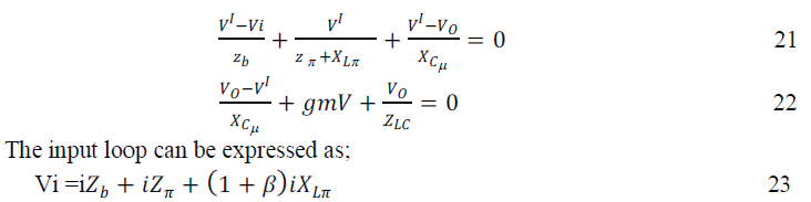 |
| Where |
| Vi is the input voltage, Vo is the output voltage, V' is the nodal point, Zb is the input impedance resonating at f1, Zπ is the impedance at rπ and Cπ, |
| ZLC is the output resistance resonating at both series (f1) and parallel resonator (f2) gm is the transconductance of the transistor (see data sheet),Lb is the base inductor, Cb is the base capacitor; Cμ is the capacitor operationg at high frequency, Lπ is the tuning inductor, Xlb,Xcb and Xπ are the impedance at lb,cb and Cπ respectively. L1and C1 is inductor and capacitor in series resonator. L2 and C2 are inductor and capacitor in parallel resonator |
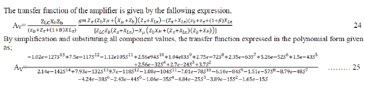
| The transfer function of the amplifier is given by the fallowing expression, |
 |
DUAL DETECTION
|
| In this case a single oscillator is used to generate 900MHz of carrier signal. An interesting effect that results from choice of the single LO Frequencies is in-band leakage to the antenna. That is, if fLO1 =900MHz is mixed with fLO2 = 1800MHz, both 900MHz and 1.8GHz components are generated at the receiver output, fLO2 is generated using frequency multiplier circuit. At the output of the multiplier a single stage filter is designed, to filter 1800MHz. This will help to further smooth the doubling output. . Fig. 6 below show the frequency doubling circuit. |
| In the above circuit full wave rectifier is used to double the given frequency, with RF centered tape transformer and BAT54C schottky diode [15]. |
| The Schottky diode diode possesses two unique features as compared to an ordinary P-N junction diode. It is unipolar device because it has electrons as the majority carrier on both side of the junction. An ordinary P-N junction diode is a bipolar device because it has both electrons and hole as the majority carriers. Since no holes are available in metals, there is depletion layer or stored charged to worry about. Hence, schottky diode can switch off faster than bipolar diode. Because of these qualities, schottky diode can easily rectify signal of frequency exceeding 300MHz. [15] |
| Frequency multiplication can also be done using bridge rectifier with a capacitor and an ordinary diode, but the above method is better. Resistors in ( kΩ) were used across the output to obtain large voltage drop. At the receiving end, the same information can be received at different frequencies. |
RESULTS
|
| The output of Dual Band-band pass filter is obtained below; |
| The model was simulated using sinusoidal input signal. When dual signal of f 1 at centre frequency of 900MHz and 1800MHz is received, the signal will pass through a dual band-band pass filter (BPF) to select the desired frequency and block the others. |
| The two filters were arranged in parallel to obtain dual band characteristics as can be seen in the fig. 7 above. |
| The transfer function of the amplifier is further simplified to obtained poles of frequencies, which are used to plot a graph with a peak at 900MHz and 1800MHz. By turning the inductor Lπ. The Figure 9 below shows the transfer function curves. |
| The figure above show the transfer function curved. A peak at 900MHz and 1800MHz.this implies that at all poles; it amplified only at desired frequencies using LC resonance circuit at the output of the amplifier. |
| The above figure indicates the magnitude of frequency doubling at 900MHz to 1.8G. |
CONCLUSIONS
|
| We are able to demonstrate that the replacement of two oscillators with a single one is feasible in the detection section of the Hajimiri architecture. The architecture is found to be feasible with additional advantages of low power consumption, light and small chip area. This result implies that, the problem of channel condition can be reduced if this architecture is adopted at both transmission and receptions points. |
Figures at a glance
|
 |
 |
 |
 |
 |
| Figure 1 |
Figure 2 |
Figure 3 |
Figure 4 |
Figure 5 |
 |
 |
 |
 |
| Figure 6 |
Figure 7 |
Figure 8 |
Figure 9 |
|
References
|
- Abu-Hundrouss, A. and. Lancaster,M .Design of multiple- band microwave filters using cascaded filter elements," Journal of ElectromagneticWaves and Applications, Vol. 23, No. 16, pp2109 - 2118.,2009
- Amplifier, IEEE microwave and wireless components letters, vol. 15, no. 10, 2005
- Department of the Army, Communications- Electronics, Fundamentals: Wave Propagation, Transmission Lines, and Antennas Headquarters, ,Washington, DC, 15 July 2004
- Donald, k. and Weaver, JR. A Third Method of Generation and Detection of for Wireless Applications,” ISSCC Digest, pp. 224-5, Feb. 1999.
- Fong, k.“Dual-Band High-Linearity Variable-Gain Low-Noise Amplifiers for wireless applications, ISSCC Digest,pp.224-5,Feb.1999.
- Hossein, H. And Hajimiri,A, Concurrent Dual-Band CMOS Low Noise Amplifiers and Receiver Architectures, IEEE Symposium on VLSICircuits Digest of Technical Papers,pp1-4.2001
- Hossein,H. Sahoolizadeh,B. Alishir,M. Moradi,N. Kordalivand,K. and Zargham Heidari, Design and Simulation of Low Noise Amplifier Circuit for 5 GHz to 6 GHz World Academy Of Science, Engineering And Technology,pp99-102,2009.
- Hossein. H and Hajimiri,A “Concurrent Multiband Low-Noise Amplifiers– Theory, Design, and Applications,” IEEE Trans. Microw. TheoryTech., vol. 50, no. 1, pp. 288–301, Jan. 2002.
- Hung L, member, IEEE, hung H, student member, IEEE, and Wang Y.. A Compact 2.4/5.2-Ghz CMOS Dual-Band Low-Noise Amplifier. IEEEMicrowave and Wireless Components Letters, vol. 15, no. 10,pp 685 October 2005
- Infenion, Data Sheet Maximum RF Input Power of SiGe:C Bipolar Transistor BFR740L3RH, , 20. Auguest 2009
- Jaldi,M. and Tayarni,M.Design of Ultra Wideband Bandpass Dual Band Filter Using Defected Ground Structures) International Journal ofInformation and Electronics Engineering, Vol. 3, No. 1, January 2013
- Ma, P., anada, T. and Hagiwara, G. Design of microstrip dual-band band pass fillter with controllable bandwidth," Microw. Optical Tech.Letters, Vol. 49, No. 3, 740{742, Mar. 2007.
- Rosenbaum, G. RF Capacitive-Coupled Filters. Applied Microwave & Wireless.glen.var@specastro.com. Vol. 3,No 3 pp 74-83,October 1998
- Ryynanen,J.“A Dual-Band RF Front-End for WCDMA and GSM Applications, CICC Digest of Technical papers, pp 175-8, May 2000 chard2002 edition pp.1743
- Verve. z , Handbook of Filter Synthesis, pp. 347-350
- Wu,S and Razavi,B. “A 900-MHz/1.8-GHz CMOS receiver for dualband applications,” IEEE.J. Solid-State Circuits, vol. 33, no. 12, pp.1-8,1998.
- D. K. Weaver, “A Third Method of Generation and Detection of Single Sideband Signals,” Proc. IRE, vol. 44, pp. 1703-5, Dec. 1956.
|