INTRODUCTION
|
| Portable multimedia and communication devices have experienced explosive growth recently. Longer battery life is one of the crucial factors in the widespread success of these products. As such, low-power circuit design for multimedia and wireless communication applications has become very important. In many such products, multi-bit flipflops and delay buffers (line buffers, delay lines) make up a significant portion of their circuits [1]–[3]. Such serial access memory is needed in temporary storage of signals that are being processed, e.g., delay of one line of video signals, delay of signals within a fast Fourier transform (FFT) architectures [4], and delay of signals in a delay correlator [2]. Currently, most circuits adopt static random access memory (SRAM) plus some control/addressing logic to implement delay buffers. For smaller-length delay buffers, shift register can be used instead. The former approach is convenient since SRAM compilers are readily available and they are optimized to generate memory modules with low power consumption and high operation speed with a compact cell size. The latter approach is also convenient since shift register can be easily synthesized, though it may consume much power due to unnecessary data movement. |
| Besides, for a design when considering power consumption, smaller flip-flops are replaced by larger multi-bit flip-flops, device variations in the corresponding circuit can be effectively reduced. |
| As CMOS technology progresses, the driving capability of an inverter-based clock buffer increases significantly. The driving capability of a clock buffer can be evaluated by the number of minimum-sized inverters that it can drive on a given rising or falling time. Fig. 1 shows the maximum number of minimum-sized inverters that can be driven by a clock buffer in different processes. Because of this phenomenon, several flip-flops can share a common clock buffer to avoid unnecessary power waste. However, the locations of some flip-flops would be changed after this replacement, and thus the wire lengths of nets connecting pins to a flip-flop are also changed. To avoid violating the timing constraints, we restrict that the wire lengths of nets connecting pins to a flip-flop cannot be longer than specified values after this process. Besides, to guarantee that a new flipflop can be placed within the desired region, we also need to consider the area capacity of the region. |
MULTI BIT FLIP-FLOPCONCEPT
|
| In this section, we will introduce multi-bit flip-flop conception. Before that, we will review single-bit flip-flop. Figure 2 shows an example of single-bit flip-flop. A single-bit flip-flop has two latches (Master latch and slave latch). The latches need “Clk” and “Clk’ ” signal to perform operations, such as Figure2 shows. |
| In order to have better delay from Clk-> Q, we will regenerate “Clk” from “Clk’”. Hence we will have two inverters in the clock path. Figure 3 shows an example of merging two 1-bit flip-flops into one 2-bit flip-flop. Each 1- bit flip-flop contains two inverters, master-latch and slave-latch. |
| Due to the manufacturing rules, inverters in flip-flops tend to be oversized. As the process technology advances into smaller geometry nodes like 65nm and beyond, the minimum size of clock drivers can drive more than one flip-flop. |
| Merging single-bit flip-flops into one multi-bit flip-flop can avoid duplicate inverters, and lower the total clock dynamic power consumption. The total area contributing to flip-flops can be reduced as well. By using multi-bit flip-flop to implement ASIC design, users can enjoy the following benefits: |
| • Lower power consumption by the clock in sequential banked components |
| • Smaller area and delay, due to shared transistors and optimized transistor-level layout. |
| • Reduced clock skew in sequential gates |
| Figure 4 shows an example of dual-bit flip-flop cell. It has two data input pins, two data output pins, one clock pin and reset pin. Use dual-bit flip-flop can get the benefits of lower power consumption then single-bit, and almost no other additional costs to pay. |
| Figure 5 shows the true table of dual-bit flip-flop cell. We could find that when CK is positive edge, the value of Q1 will pass to D1, and the value of Q2 will pass to D2. Or Q1 and Q2 will keep original value. |
MULTI BIT FLIP-FLOP METHODOLOGY
|
| In the section, we will introduce that how to use Design Compiler and Faraday’s multi-bit flip-flop to implement ASIC design. |
| A) The criteria of using multi-bit flip-flop |
| Multi-bit flip-flop cells are capable of decreasing the power consumption because they have shared inverter inside the flip-flop. Meanwhile, they can minimize clock skew at the same time. |
| To obtain these benefits, the ASIC design must meet the following requirements. The single-bit flip-flops we want to replace with multi-bit flip-flop must have same clock condition and same set/reset condition. When you set the variable hdlin_infer_multibit as default_all, Design Compiler will use multi-bit flip-flop to replace bus type single-bit flip-flops. For non-bus condition, your must use create_multibit to identify the multi-bit flip-flop candidates. |
MEMORY ORGANIZATION BETWEEN EACH MODE
|
| In the proposed memory organization, several power reduction techniques are adopted. Mainly, these circuit techniques are designed with a view to decreasing the loading on high fan-out nets, e.g., clock and read/write ports. |
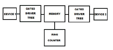 |
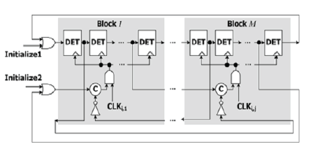
| A) RING COUNTER |
| This ring counter proposed to replace the R–S flip-flop by a C-element and to use tree-structured clock drivers with gating so as to greatly reduce the loading on active clock drivers. Additionally, DET flip-flops are used to reduce the clock rate to half and thus also reduce the power consumption on the clock signal. The proposed ring counter with hierarchical clock gating and thecontrol logic is shown in above figure. Each block contains one C-element to control the delivery of the local clock signal “CLK ”to the DET flip-flops, and only the “CKE signals along the path passing the global clock source to the local clock signal are active. The “gate” signal (CKE ) can also be derived fromthe output of the DET flip-flops in the ring counter. The C-element is an essential element in asynchronous circuits for handshaking. |
 |
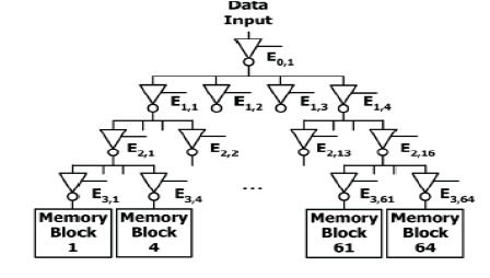
| B) GATED DRIVER TREE |
| To save area, the memory module of a delay buffer is often in the form of an SRAM array with input/output data bus as in [6]. Special read/write circuitry, such as a sense amplifier, is needed for fast and low-power operations. However, of all the memory cells, only two words will be activated: one is written by the input data and the other is read to the output. Driving the input signal all the way to all memory cells seems to be a waste of power. |
| The same can be said for the read circuitry of the output port. In light of the previous gated-clock tree technique, we shall apply the same idea to the input driving/output sensing circuitry in the memory module of the delay buffer. The memory words are also grouped into blocks. Each memory block associates with one DET flip-flop block in the proposed ring counter and one DET flip-flop output addresses a corresponding memory word for read-out and at the same time addresses the word that was read one-clock earlier for write-in. |
 |
RESULTS
|
 |
 |
CONCLUSION
|
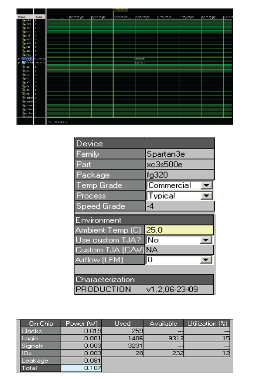
| Using Multi-Bit Flip-flop in combination with gated tree drive is an effective and efficient implementation methodology to reduce the power consumption by merging single-bit flip-flop. In this paper, we have implemented design with XILINX Design Compiler and Faraday’s multi-bit flip-flop. Experimental results indicate that multi-bit flip-flop is very effective and efficient method in lower-power designs. We will use this methodology to implement real ASIC project in the future. |
Figures at a glance
|
 |
 |
 |
 |
 |
| Figure 1 |
Figure 2 |
Figure 3 |
Figure 4 |
Figure 5 |
|
References
|
- Ya-Ting Shyu, Jai-Ming Lin, Chun-Po Huang, Cheng-Wu Lin, Ying-Zu Lin, and Soon-Jyh Chang “Effective and Efficient Approach for Power Reduction by Using Multi-Bit Flip-Flops”IEEE TRANSACTIONS ON VERY LARGE SCALE INTEGRATION (VLSI) SYSTEMS
- P. Gronowski, W. J. Bowhill, R. P. Preston, M. K. Gowan, and R. L.Allmon, “High-performance microprocessor design,” IEEE J. Solid-StateCircuits, vol. 33, no. 5, pp. 676–686, May 1998.
- W. Hou, D. Liu, and P.-H. Ho, “Automatic register banking for low-power clock trees,” in Proc. Quality Electron. Design, San Jose, CA,Mar.2009, pp. 647–652.
- Eberle.W et al 2001 80-Mb/s QPSK and 72-Mb/s 64-QAM flexible and scalable digital OFDM transceiver ASICs for wireless localarea networks in the 5-GHz band IEEE J. Solid-State Circuits, vol. 36, no. 11, pp. 1829–1838.
- Hosain.R, L. D. Wronshi, and albicki.A, 1994. Low power design using double edge triggered flip-flop,” IEEE Trans. Very Large ScaleIntegr. (VLSI ) Syst., vol. 2, no. 2, pp. 261–265.
|