Keywords
|
| AES CORE, FPGA, Verilog HDL, DES |
INTRODUCTION
|
| Cryptography has existed in one form or another for thousands of years. From analyzable codes, comprised of numbers and text to unperceivable forms, encryption has played a key role in communication throughout the ages. Encryption played its role in protecting sensitive texts, messages by making them to highly classified. The term Caesar Cipher take us centuries back, so that one can imagine the current age of cryptography. Though this centuries old cipher is now so simple for us to break. But over the time numerous theories, models and structures proposed for different cryptographic techniques. In modern days, mathematical theory and computational hardware practices have significant impact on cryptographic algorithms making them hard to intercept by any antagonist practically, though on paper it seems breakable. |
| Modern cryptography intersects the disciplines of mathematics, computer science and engineering. Cryptography finds wide application areas from individuals’ data secrecy to defence communication to e-Commerce to network security. |
HISTORY
|
| The Advanced Encryption Standard (AES) for the encryption of electronic data established by the U.S. National Institute of Standards and Technology (NIST) in 2001.It is based on the Rijndael cipher developed by two Belgian cryptographers, Joan Daemen and Vincent Rijmen, who submitted a proposal which was evaluated by the NIST during the implementation of Federal Information Processing Standards Publications (FIPS PUBS). The U.S. government adopted AES initially, now being used globally over worldwide communication networks. It supersedes the Data Encryption Standard (DES), which was published in 1977 [1]. |
| The Data Encryption Standard (DES) was about to expire in 1998, so National Institute of Standards and Technology (NIST) formerly National Bureau of Standards (NBS), initiated a process to develop a Federal information Processing Standard (FIPS) for the Advanced Encryption Standard (AES), specifying an Advanced Encryption Algorithm to replace the Data Encryption standard (DES) the Expired in 1998. NIST has solicited candidate algorithms for inclusion in AES, resulting in fifteen official candidate algorithms MARS, RC6, Rijndael, Serpent and Two fish of which Rijndael was chosen as the Advanced Encryption Standard [1], [4], [6]. |
| The AES algorithm is a symmetric block cipher that can encrypt, (encipher), and decrypt, (decipher), information. Encryption converts data to an unintelligible form called cipher-text. Decryption of the cipher-text converts the data back into its original form, which is called plaintext. The AES algorithm is capable of using cryptographic keys of 128, 192, and 256 bits to encrypt and decrypt data in blocks of 128 bits [5]. |
METHODOLOGY
|
| The AES algorithm [2] allows input and output data sequences of 128 bits. These sequences are referred to as blocks and the numbers of bits they contain are referred to as their length. The Cipher Key for the AES algorithm may be of 128, 192 or 256 bits in length. Other input, output and Cipher Key lengths are not permitted by this standard. The bits within such sequences are numbered starting at zero and ending at one less than the sequence length, which is also termed the block length or key length. The number i attached to a bit is known as its index and will be in one of the ranges 0 ≤ i <128, 0 ≤ i < 192 or 0 ≤ i < 256 depending on the block length or key length specified. |
| All byte values in the AES algorithm are presented as the concatenation of the individual bit values, (0 or 1), between braces in the order {b7, b6, b5, b4, b3, b2, b1, b0}. These bytes are interpreted as finite field elements using a polynomial representation |
 |
| Internally, the AES algorithm’s operations are performed on a two dimensional array of bytes known as the State [2]. The State consists of four rows of bytes. Each row of a state contains Nb numbers of bytes, where Nb is the block length divided by 32. In the State array, which is denoted by the symbol S, each individual byte has two indices. The first byte index is the row number r, which lies in the range 0 ≤ r ≤ 3 and the second byte index is the column number c, which lies in the range 0 ≤ c ≤ Nb−1. Such indexing allows an individual byte of State to be referred to as Sr, c or S[r, c]. For the AES Nb = 4, which means that 0 ≤ c ≤ 3. At the beginning of the Encryption and Decryption the input, which is the array of bytes symbolized by {in0in1???in15} is copied into the State array. This activity is illustrated in Figure below. The Encryption or Decryption operations are conducted on the State array. After manipulation of the state array has completed its final value is copied to the output, which is an array of bytes symbolized by {out0out1???out15} [2], [3], [5]. |
| At the beginning of the cipher, the input array is copied into the State according the following scheme- S[r, c] = in [r + 4c] for 0≤ r≤ 3 & 0≤ c ≤3, and at the end of the cipher the State is copied into the output array as shown below- out[r+4c] = s[r, c] for 0≤ r≤ 3 & 0≤ c≤ 3. |
| A. Encryption |
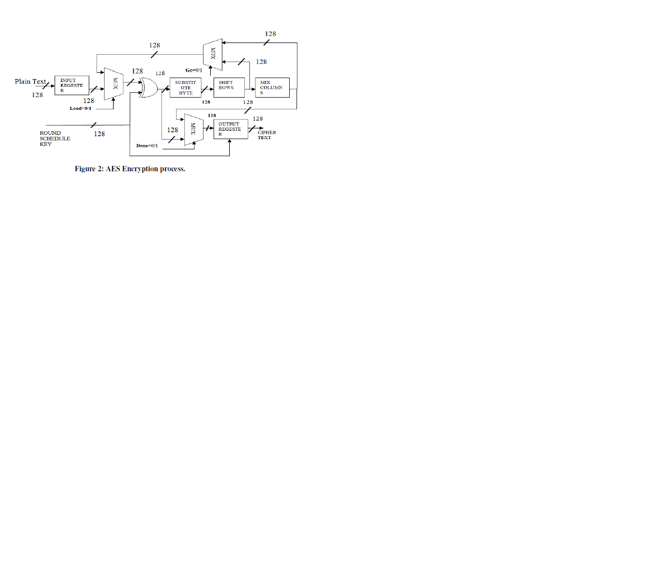
| During encryption 128 bit plain text is enciphered, round key scheduled and produces the encrypted cipher text – 128 bit depending on the control signals as follows, i.e., In Encryption mode, Load pin is given logic ‘1’, 128 bit plaintext will be loaded. Reset will be made logic ‘1’, after loading the data. After the end of 10 rounds of internal blocks, Sub bytes, shift rows and mix column processing, done signal will go to logic ‘1’ state and output register, now holds the encrypted output. |
| B. Decryption |
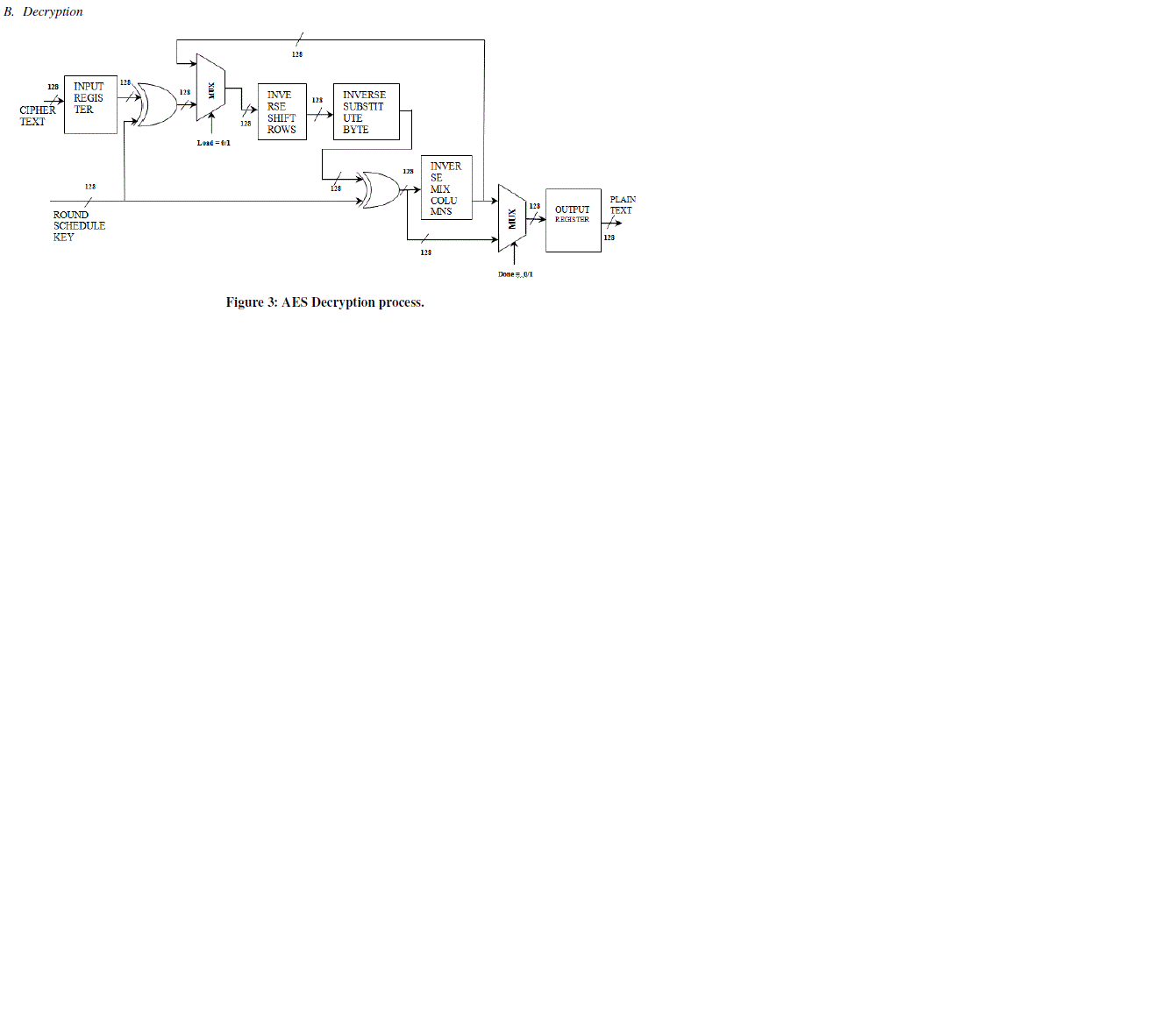
| The decryption block processes the cipher text (128 bit) & encrypted key (128 bit), obtained in the final stage encryption and reproduces the original data as decrypted output (128 bit) along with the 128 bit key. The control signal Load will be forced to logic ‘1’ to load Encrypted 128 bit data and 128 bit key schedule and reset is made logic ‘1’ after loading the inputs & then load is made logic ‘0’ and finally the process of decryption continues for 10 rounds to decrypt the data. |
| C. Verilog Implementation |
| The Verilog HDL, the most popular rather simpler than VHDL (VHSICHDL) is an IEEE standard hardware description language. It is widely used in the design of digital integrated circuits. Basically Verilog is verification through simulation, for timing analysis, for test analysis and for logic synthesis. Verilog HDL allows designers to design at various levels of abstraction like register transfer level, gate level and switch level. Verilog is used as an input for synthesis programs which will generate a gate-level description for the circuit. Xilinx ISE 13.2 is a software tool developed by Xilinx for synthesis and analysis of HDL designs [7]. |
| D. FPGA Implementation of the Design |
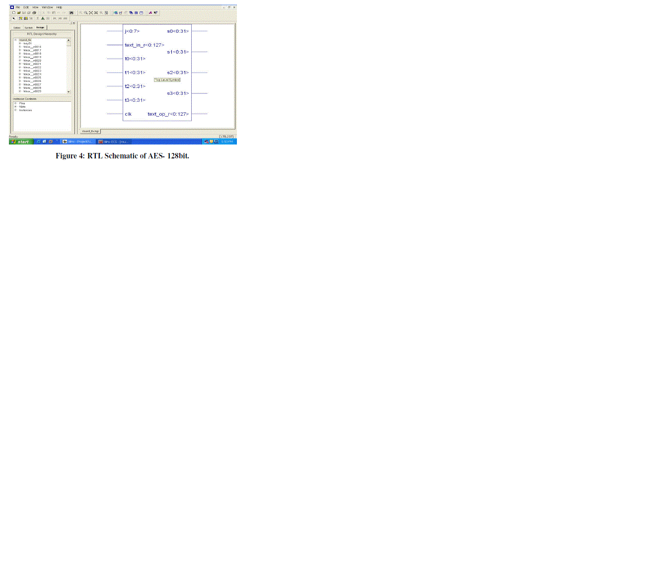
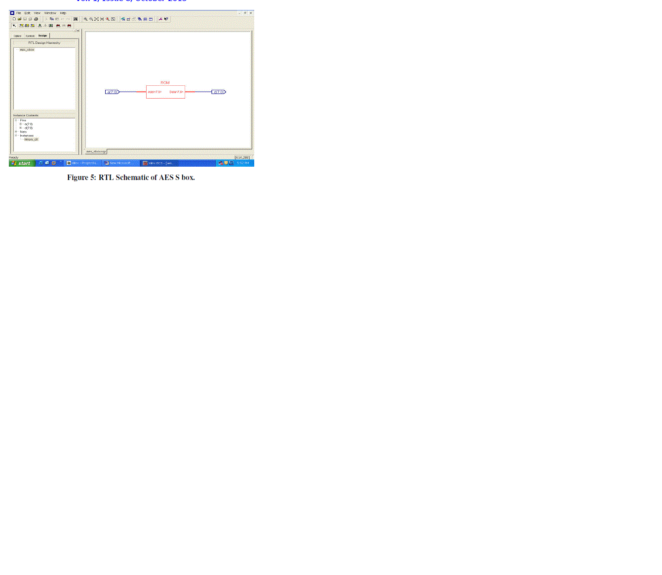
| Figure 4 shows the RTL schematic of AES-128 bit which comprises of AES Encryption and Decryption, while the Figure 5 depicts RTL schematic of ROM which further treated as AES- S Box. |
SIMULATION RESULT USING MODELSIM
|
| Figure 6 shows the simulation results using Model Sim for AES-128 bit by considering the following inputs. |
| Input data – 0123456789abcdeffedcba0123456789; |
| Encryption key – cc9730602009ea9503103666fd864888; |
| The Encrypted output obtained is as shown. |
| Received data –89ff1abd4226257381330dbcce6e8810; |
| Decryption Key –919503103782df80a8c7bbe534d2ce02; |
| The hardware utilization by various devices during AES Encryption is represented in tabular sheet which includes modules like Add Round Key, Schedule Substitute Byte. |
| Following table summarizes the utilization of various devices while decrypting the data; consisting of Add Round Key module, Schedule Inverse-Substitute Byte module and Inverse- Mix Column module. |
CONCLUSION
|
| In this way the above proposed work i.e. AES core supports both encryption and decryption standards. Xilinx simulation tool used to verify the design and in response it is concluded that with FPGA (from Spartan family)target device, design uses 2439 slices, 2252 flip flops, 4229 4- input look up tables and operates at 2.97 Gbps (Throughput). |
| This AES core implementation using Rijndael algorithm for 128 bit data blocks with its far better results than its other opponents encourages the cryptographic standard to focus on to even larger data blocks of lengths like 192 bits, 256 bits of plain text data and to go further with appropriately selected key lengths, in order to achieve the best cryptographic algorithm so that adversaries, intruders are kept away from sensitive information. |
ACKNOWLEDGMENT
|
| The authors would like to thanks all the management and faculties of SES Shaaz college of Engineering for their generous, moral and technical support throughout the completion of this work. We also acknowledge all those individual brains and hands around, to make it into a complete work, without them this task would never turn out to be complete. |
Tables at a glance
|
 |
 |
| Table 1 |
Table 2 |
|
Figures at a glance
|
 |
 |
 |
| Figure 1 |
Figure 2 |
Figure 3 |
 |
 |
 |
| Figure 4 |
Figure 5 |
Figure 6 |
|
References
|
- National Institute of Standards and Technology, “Announcing the Advanced Encryption Standard (AES)”, Federal InformationProcessing Standards Publication 197, pp. 1-47, 26 November 2001.
- J.Daemenand, V.Rijmen, “AES Proposal: Rijndael”, Document version 2, pp. 1-45, 3 September 1999, http://csrc.nist.gov/cryptotoolkit/AES/Rijndael/Rijndael.pdf
- M. M. WONG, M.L.D. Wong, “A high throughput low power compact AES s-box implementation using composite field arithmetic and algebraic form representation”, proc. IEEE 2nd Aseasymposium on quality electronic design, pp 318-323, 2010.
- Monica libertori, Fernando Otero, J.C.Bonadero, Jorge Castineira, “AES-128 Cipher High Speed, Low Cost FPGA Implementation”, 3rd
- Southern Conference on Programmable Logic, Institute of Electrical and Electronics Engineers xplore, ISBN:1-4244-0606-4, pp.195-198, April 2007.
- Leelavathi.G, Prakasha S, Shaila K, Venugopal K R, L M Patnaik, “Design and Implementation of Advanced Encryption Algorithm withFPGA and ASIC”, International Journal of Research in Engineering & Advanced Technology, Volume 1, Issue 3, ISSN: 2320 –8791, pp.1-8, June-July, 2013.
- M.Matsui, “Linear cryptanalysis method for DES cipher”, Springer, Eurocrypt, Lncs765, pp.386-397, 1994.
- Samir Palnitkar, “Verilog HDL- A Guide to Digital Design and Synthesis”, Prentice Hall, pp. 3-10, 2003.
|