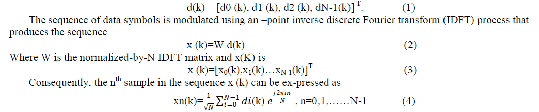
In this paper, we present a novel design for the detection of primary synchronization signal in a Long Term Evolution (LTE) system based device at the expense of low cost and low power. This is facilitated by using a matched filter architecture which incorporates parallel processing. The approach of a 1-bit analog-to-digital converter (ADC) with down-sampling is compared with that of a 10-bit ADC without down-sampling under multi-path fading conditions defined in LTE standard for user equipment (UE) performance test. A high performance primary synchronization signal detection method is derived in this paper.
Keywords |
| Low cost, low power, matched filter, primary synchronization signal (PSS). |
INTRODUCTION |
| The LTE, also referred as EUTRA (Evolved UMTS Terrestrial Radio Access), is intended to enhance the 3g and
3.5g systems in order for them to adopt higher peak data rates with extremely high mobility support. The LTE, as one
of the latest steps in an advancing series of mobile telecommunications system, can be seen to provide a further
evolution of functionality, increased speeds and general improved performance comparing to the third generation
systems [1].The LTE specification provides downlink peak rates of at least 100 Mbps, and uplink of at least 50 Mbps.
Synchronization sequence is more important because its detection affects not only search time but also performance of
demodulation. The 3GPP working group decided to adopt Zadoff-Chu (ZC) sequences as the downlink primary
synchronization signal (PSS) and the uplink random access preamble. A Zadoff-Chu sequence is a complex-valued
mathematical sequence which exhibits the useful property that cyclically shifted versions of it are orthogonal to each
other. The ZC sequences have flat frequency domain autocorrelation property and the low frequency offset sensitivity
[5]. The primary synchronization signal is detected by using a non coherent detection method since there is no
reference information initially. The main objective of this paper is to propose an efficient matched filter architecture
that involves less number of complex multiplications to occur. The system model and PSS definition are presented in
Section II. A brief review of the matched filter approach is presented in Section III. Afterwards, both the method of 1-
bit ADC with down-sampling and that of 10-bitADC without down-sampling for PSS detection are discussed in
Section IV. Section V addresses different implementation architectures of PSS detection. Whereas their simulation
results are shown in Section V1 Finally, conclusion remarks are given in Section VII. |
SYSTEM MODEL AND PROBLEM DEFINITION |
| A. OFDM System Model with Carrier Frequency Offset (CFO) |
| 3GPP adopt OFDM to improve spectrum efficiency. In OFDM systems, a sequence of complex data symbols is
considered as orthogonal subcarriers during the k th OFDM blocks, the sequence of data symbols is defined as follows: |
 |
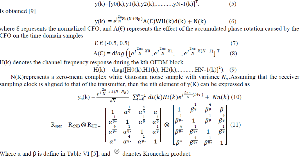
| In fading channels, a time-domain guard interval, which is named as cyclic prefix (CP), is created by copying the
last samples of the IDFT output and appending them at the beginning of the OFDM symbol to be transmitted. So the
transmitted OFDM block consists of (N + Ng) samples [7].At the receiver side, after removing the first CP samples, the
received sequence |
 |
| B. PSS |
| The P-SCH is used for obtaining the time and frequency synchronization necessary for demodulating the S-SCH
[6]. The UE achieves synchronization by correlating the received P-SCH signal with a replica of the transmitted signal
(i.e., using a matched filter), thereby identifying a correlation peak at the proper symbol timing. The Primary
Synchronization Signals are modulated using one of three different frequency domain Zadoff-Chu sequences. The
sequence du (n) used for the PSS is generated from a frequency-domain ZC sequence [1] according to |
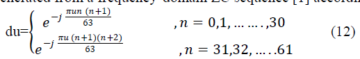 |
| Where the ZC root sequence index is given by Table II |
| The three different ZC sequences are orthogonal to each other, and each sequence corresponds to a sector identity
which is in the range of 0 to 2. The Primary Synchronization signal first determines one of three cell identities (0, 1, 2),
also represented by N (2) ID. Then the secondary synchronization signal is used to determine a cell ID between 0 and
167 represented by N (1) ID. A Zadoff-Chu sequence is a complex-valued mathematical sequence which exhibits the
useful property that cyclically shifted versions of it are orthogonal to each other. Thus, it is easy to detect PSS during
the initial synchronization because the ZC sequence has the flat frequency domain autocorrelation property and the low
frequency offset sensitivity. |
FUNDAMENTAL OF PSS DETECTION |
| The main function of PSS is to detect the boundary of a frame where non-coherent detection method has to be used
at the receiver since there is no known reference information initially [7]. Matched filter is a basic non-coherent
detection method that can be used to detect PSS efficiently. The sequence in (12) is mapped to the subcarriers around
DC and transformed to time domain by 64-point IDFT. To detect this signal at the receiver, the correlation with the
time domain signal of the ZC sequence is calculated [2]–[4]. |
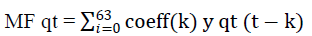
| Cu(m)=(WH du)Hy (13) |
| Where y is the successive 64-by-1 received signal vector, is the DFT matrix, and is 64-by-1 vector composed of
punctured at DC. |
| Then, from (13), the coefficients of the matched filter can be obtained |
| Coeff= (WH du)H (14) |
| Where |
| Coeff= [Coeff(63)Coeff(62).......Coeff(1)Coeff(0)] (15) |
| and the matched filter can be expressed |
 (16) (16) |
| Where y (k) is the received signal. |
PROPOSED DESIGN OF PSS |
| The receiver side of an OFDM system model ADC is present for digital representation of the received signal. 10-
bit ADC is generally preferred to be used at the receiver. From the power consumption perspective, a 10-bit analog-to
digital converter (ADC) uses more power than 1-bit ADC. Typically, the power consumption of a 1-bit 122.88 MHz
ADC composed of one comparator is about 200 W, while the power consumption of a 10-bit 122.88 MHz pipelined
ADC is about 50mW. |
| To come up with a low-power solution, a method of PSS detection using 1-bit ADC is proposed.PSS is transmitted
periodically, twice per frame which lasts 10 ms [8]. The sampling rate of the receiver is 122.88 MHz; however, the date
rate of input data to the matched filter is 1.92 MHz Thus, 9600 samples at the output of the matched filter need to be
buffered during the 5 ms period, which is not area and cost efficient. To come up with a low cost solution, a method of
down-sampling by 8 is used at the output of matched filter. |
| A. Method without Down-Sampling by 8 for 10-Bit ADC |
| From the last section, the matched filter as expressed in (16) can be reformulated when using a 10-bit, 122.88 MHz
pipelined ADC |
 |
| where yqt(k) is the received signal sampled by a 10-bit, 122.88 MHz pipelined ADC, and is obtained in (14) and
(15).Every output of the matched filter is buffered since there is no down-sampling module, and it needs a large area
buffer which is very costly. |
| B. Method With Down-Sampling by 8 for 1-Bit ADC |
| Equation (16) can be reformulated when using a 1-bit, 122.88 MHz ADC |
 (18) (18) |
| Where yqo (k) is the received signal sampled by a 1-bit, 122.88MHz ADC, and is obtained in (14) and (15).Every
output of the matched filter is down-sampled by 8 |
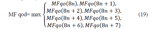 |
| where MFqod is the output of the down-sampling module. Now, only 1200 outputs need to be buffered during 5 ms
with an additional comparator of 1 out of 8 implementing the down sampling module. This results in less area which
translates to lower cost in a practical system. Its implementation architecture is discussed in next chapter [12]. |
HARDWARE IMPLEMENTATION |
| The implementation architecture of the proposed method is presented here along with the new matched filter
architecture that reduces the complexity involved in existing methodology. The matched filter is an important
component in the PSS detection. We use 64-tap time domain matched filter; hence 64 complex multiplication units per
matched filter are used in the calculation in [16]. |
| A. Existing Architecture of Matched Filter |
| In this architecture input data that is being received is processed serially. As per our simulation assumptions, 84
matched filters are required in the system. So a total of 5376 units of complex multiplication is needed. Instead we can
use only one complex multiplication unit during 64 cycles instead of using 64 units of complex multiplication. As a
result, 84 units of complex multiplication are enough for the whole system. But the problem that it encounters is that
since the data is processed serially, so significant amount of delay is encountered due to the shifting involved in it. This
problem is overcome in our proposed method [19]. |
| B. Architecture of PSS Detection |
| A mismatch of up to 14 part per million (ppm) can exist between the oscillators at the eNodeB and at the UE, so
seven groups of matched filters are used to cover the range of 14 ppm, 14 ppm. Each group contains three matched
filters to detect three different physical-layer IDs of value 0, 1, or 2 [21]. Therefore, there are 21 hardware units as
shown in Fig. 2 for each receiver antenna. Since the system is MIMO 4-by-4 and there are 4 receiver antennas at the
UE end, 84 such hardware units are involved in the architecture of the PSS detection. A total of 9600 samples during 5
ms and thus a single port RAM with 9600 addresses is needed.
As described above, there are 84 such RAMs in the system, and the area is too large for the UE chip; therefore an
area efficient architecture is proposed as shown in Fig. 2. Compared to the architecture in Fig. 1, a small RAM with 8
addresses is added whose function is to find the maximum value of every eight correlations. As a result, only 1200
correlation values need to be stored in RAM with 1200 addresses, which reduce the RAM size of the whole system by a
factor of almost 8 [22]. We can observe that the area of the area-efficient architecture is much smaller than that of the
original architecture, which reduces the Cost of the chip significantly. From the power perspective, not only the 1-bit
ADC reduces the power consumption, but the hardware of digital logic also does. |
SIMULATION RESULTS |
| Primary synchronous signal is designed for cell search and handover in 3GPP LTE systems, which is transmitted
every 5ms. Search time of PSS detection is an important criterion when measuring its performance. To compare the
performance using a 10-bit 122.88MHz ADC without down-sampling and that using a 1-bit 122.88MHz ADC with
down-sampling by 8, the parameters listed in Table III are used in the simulation [23].The simulation results for search
time of both the methods under EPA 5 Hz channel model are shown. It is clear that the search time of both methods
under EPA 5 Hz model with low correlation channel matrix, is very close to each other. The Existing and the proposed
model is simulated using altera quartus software.The power and gate analysis are carried out for both the methods.The
simulation results show that the performance of our proposed matched filter architecture which incorporates parrellel
processing is efficient in terms of power [24]. Furthermore,the implemenation of our proposed architecture with the
method of 1-bit adc with down sampling by a factor of 8 results in the reduction of overall gates required for it to be
implemented in the user equipment.This is shown in table V. |
PERFORMANCE WITH EXISTING STATE-OF-THE-ART MATCHED FILTER ARCHITECTURE |
| The matched filter architecture, in the design [4] uses 84 matched filters and 5376 units of complex multiplication
making the practical implementation difficult. The matched filter architecture in the design [22] requires only 84 units
of complex multiplication and this is practically possible. But the cost for implementation is high. In the design [40],
the matched filter architecture uses a serial mechanism and consumes more logic elements. The proposed architecture is
power and area efficient. In the proposed matched filter architecture, a parallel mechanism is used for inputting the data
and the logic elements utilized is also significantly reduced. One bit ADC with down sampling by factor 8 consumes
339896 Kilo Byte and the power utilized is less when compared to design [40].Ten bit ADC without down sampling,
consumes 46.88Mili Watt as static power and 16.48Mili Watt as dynamic power. The logic elements utilized is also
significantly reduced when compared to the existing state of architecture. The problem with the existing architecture is,
since the data is processed serially a significant amount of delay is encountered due to the shifting involved in it. This
occurs when one value is high and subsequent values are low, no matter what the shift is, the output of the MUX will
be the same. This causes unnecessary multiplication to occur and also the delay that is involved affects the overall
performance of the system. This problem is overcome in our proposed architecture which incorporates parallel
processing. So, there is no shifting of input data during each input clock. As a result of it, the effect of propagation
delay is overcome and the table 4.6 shows the comparison with the existing state architecture. |
CONCLUSION |
| The detection of PSS plays a primary role in mobile communication. Theoretically, detection with 1-bit ADC and
with down-sampling would degrade the performance and prolong the detection time. However, due to the inherent
advantage of the ZC sequence, simulation results show that the performance of the proposed method using a 1-bit ADC
with down-sampling by 8 does not degrade much compared with that using a 10-bit ADC without down-sampling in
the presence of frequency offset under several typical LTE propagation channels. Subsequently, two different
implementation architectures of the PSS detection are presented. The area and the power consumption of the original
implementation architecture are too large. Based on the simulation results in the proposed architecture, the PSS can be
detected efficiently and accurately at a much lower power and lower cost which renders it feasible in the
implementation of a UE chip. |
FUTURE WORK |
| As first phase of the project, primary synchronization signal (PSS) is simulated using Model Sim. In the future
phase of the project, FPGA implementation is proposed to be carried and investigation of real-time performance
metrics will also be carried out. Further, detection of Secondary synchronization signal (SSS) will also be done. In case
of significant deterioration in the performance, hardware solutions will be investigated. |
Tables at a glance |
 |
|
|
|
|
| Table 1 |
Table 2 |
Table 3 |
Table 4 |
Table 5 |
|
|
|
|
| Table 6 |
Table 7 |
Table 8 |
Table 9 |
|
| |
Figures at a glance |
 |
 |
 |
 |
 |
| Figure 1 |
Figure 2 |
Figure 3 |
Figure 4 |
Figure 5 |
|
| |
References |
- B. M. Popovic and F. Berggren, “Primary synchronization signal in E-UTRA,” in Proc. IEEE 10th Int. Symposium. Spread Spectrum Technology. Applied (ISSSTA), pp. 426–430, 2008.
- 3rd Generation Partnership Project (3GPP),Sophia-Anti polis Codex, France,3GPP TS 36.211 v8.9.0 3rd Generation Partnership Project; GPP Dec.2009,.
- K. Melonakos, D. M. Gutierrez Estevez, V. Jung nickel, X. Wen, and C.Drewes, “A closed concept for synchronization and cell search in GPP LTE systems,” in Processing. IEEE Wireless Communication Network Conference. pp. 1–6, 2009.
- S. Sepia, I. Tewfik, and M. Baker, LTE-The UMTS Long Term Evolution: From Theory to Practice. New York: Wiley, 2009.
- H.-G. Park, I.-K. Kim, and Y.-S. Kim, “Efficient coherent neighbor cell search for synchronous 3GPP LTE system,” Electron. Letter, volume.44, no.21, Oct. 2008.
- Chixiang Ma, Hao Cao and Ping Lin „A Low-Power Low-Cost Design Of Primary Synchronization Signal Detection‟. IEEE Transactions On Very Large Scale Integration Systems, Vol. 20, No. 7, July 2012.
- K. Melonakos, D. M. Gutierrez Estevez, V. Jung nickel, X. Wen, and C.Drewes, “A closed concept for synchronization and cell search in 3GPP LTE systems,” in Proc. IEEE Wireless. Communication. Network. Conference, pp. 1–6, 2009.
- F. J. Harris, “Orthogonal frequency division multiplexing, OFDM,” presented at Department of Electrical Engineering, San Diego State University, San Diego, CA, 2008.
- 3GPP TS 36.101 v8.9.0 3rd Generation Partnership Project; Technical Specification Group Radio Access Network; Evolved Universal Terrestrial Radio Access (E-UTRA); User Equipment (UE) Radio Transmission and Reception (Release 8), 3rd Generation Partnership Project, Technology Representation 3GPP, December 2009.
- 3GPP. (n.d.). 3GPP TR 25.913 - v7.3.0, Requirements for EUTRA and EUTRAN Online. Available:http://www.3gpp.org/ftp/Specs/archive/25%5Fseries/25.913/
- European Telecommunications Standards Institute, 3GPP TS 36.211 version 9.1.0 Release 9, Sophia Antipolis, France: ETSI, 2010.
- G. Colavolpe and R. Raheli, “Noncoherent sequence detection,” IEEE Transaction Communication, vol. 47, no. 9, pp. 1376–1385, Sep. 1999.
- R. Van Nee, and R. Prasad, OFDM for Wireless Multimedia Communications. Norwood, MA: Artech House Publishers, 2000.
- Y. Yao and G. B. Giannakos, “Blind carrier frequency offset estimation in SISO, MIMO and multiuser OFDM systems,” IEEE Transaction Communication, vol. 53, no. 1, pp. 173–183, Jan. 2005.
- H.G. Myung, J. Lim, and D. J. Goodman, “Single Carrier FDMA for Uplink Wireless Transmission,” IEEE Vehicular Technology Society. volume. 1, no. 3, pp. 30-38, Sept. 2006.
- Mobile Cell Search And Synchronization In LTE -A Thesis Presented to the Faculty of San Diego State University by NaliniParavastuSamavedam.
- H.-G. Park, I.-K. Kim, and Y.-S. Kim, “Efficient coherent neighbor cell search for synchronous 3GPP LTE system,” Electron. Letter, volume.44, no.21, Oct. 2008.
- J.-I. Kim, J.-S. Han, H.-J. Roh, and H.-J. Choi, “PSS detection method for initial cell search in 3GPP LTE FDD/TDD dual mode receiver,” presented at the 9th International Symposium on Communications and Information Technology, Inche on, Korea, Sept. 2009.
- B. M. Popovic and F. Berggren, “Primary synchronization signal in E-UTRA,” in Processing. IEEE 10th International. Symposium Spread Spectrum Technology. Application (ISSSTA), pp. 426–430, 2008.
- 3GPP Technical Specification 32.422, „Telecommunication management; Subscriber and equipment trace; Trace control and configuration management (Release 10).
|