Keywords
|
| common mode feedback, harmonic distortion, miller compensation, fully differential. |
INTRODUCTION
|
| Fully differential circuits process signals fully-differentially without any control over the common mode potential. It is the common mode feedback (CMFB) circuit that keeps the common mode potential stable. Through the feedback action, the detected common-mode voltage is kept close to the common-mode reference voltage. There are several critical factors in designing CMFB circuits. The CM detector should not load the main opamp. The CM detector should have a larger input signal range. The interaction between the CMFB loop and the fully-differential signal processing should be minimized. The CMFB loop should be fast with a moderate to high gain. |
MILLER COMPENSATION
|
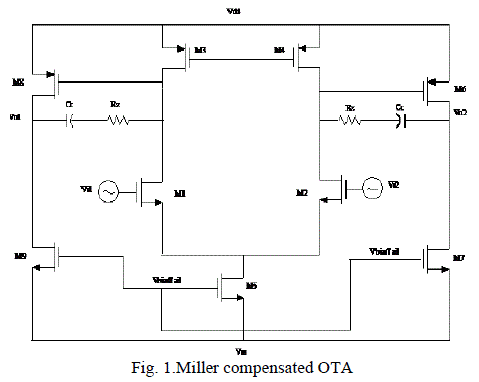
| A Fully Differential Configuration as shown in Fig.1 is used to implement the two stage OTA so as to achieve better signal swing and for better noise rejection. The gain of single stage amplifier is limited to the product of the input pair transconductance and the output impedance. To achieve more gain and better signal swing at the output we can use “two-stage” opamps, with the first stage providing a high gain and the second, large swings. |
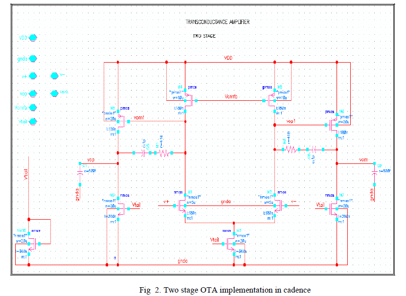
| In a two stage amplifier as shown in fig.2 , a compensation capacitor and a right half plane zero compensating resistor is connected between the two stages for stability during the feedback operation. The series resistor value is given by Rz = 1/gmp where gmp is the transconductance of the PMOS transistor of second stage. The choice of coupling capacitor is based on the phase margin required. Phase margin of 60 degrees is adequate for this design. The W/L ratios of transistors are given in Table I. |
| A. AC analysis of OTA |
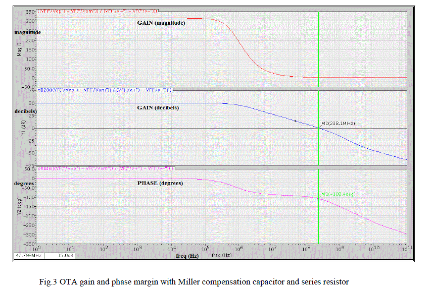
| To measure the phase margin of uncompensated OTA and compensated OTA, ac analysis was performed and the fully differential gain and phase were plotted as in fig.3. Find the unity gain frequency of the amplifier (0 dB) and find the phase at this frequency. Phase margin = 180o + phase at the unity gain frequency. Results are tabulated in Table II. |
| B. Harmonic Distortion Analysis |
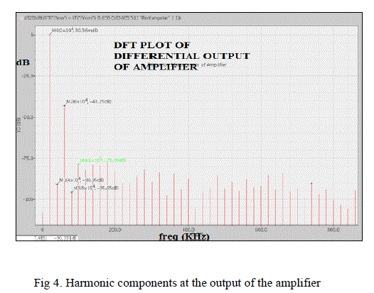
| The nonlinearity of a circuit can be characterized by applying a sinusoid at the input and measuring the harmonic component of the output. |
| From the fig.4,it can be observed that the odd harmonics are having higher magnitude than even harmonics. In a fully differential amplifier the even harmonics should be cancelled out. |
IMPLEMENTATION OF COMMON MODE FEEDBACK CIRCUIT
|
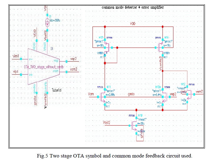
| The common mode voltage at the output of the OTA is detected by using split transistors of half the width as that of the transistor to which reference voltage 1.65 V is applied as shown in fig.5. The W/L ratios of the transistors are same as that of the OTA. The difference between the common mode voltage and Vref is amplified by the error amplifier and output current is fed back to the gate of OTA load transistors. |
| A. CMFB CIRCUIT FOR TWO STAGE OTA |
| In two stage amplifier, the common mode feedback cannot be realized as for a single stage amplifier because two inversions would occur between the feedback node and the output nodes, resulting in a positive feedback that would make the system unstable. Hence the feedback was taken from the drain of split transistors itself to give negative feedback to first stage of OTA. |
| B. Common mode response for a current pulse |
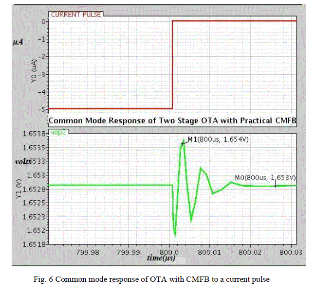
| The common mode response of fully differential OTA with common mode feedback circuit is plotted in fig.6.Output voltage is found to be 1.653 volts .The common mode response of fully differential OTA with common mode feedback circuit is plotted in fig.6.Output voltage is found to be 1.653 volts . |
DISTORTION MEASUREMENT OF TWO-STAGE OTA WITH CMFB CIRCUIT
|
| The total harmonic distortion of the fully differential OTA is found out. Results indicate that the even harmonics are having much less amplitude compared to the odd harmonics. Table III gives the summary of the DFT values of the fundamental and up to the fifth harmonic. |
CONCLUSIONS
|
| Fully Differential OTA is integrated with a common mode feedback circuit. Common mode feedback circuit was designed to stabilize the output common mode levels of the Operational Transconductance Amplifier. DFT of the differential output is measured and the values are plotted in dB. The even harmonics are of much less magnitude compared to odd harmonics because of fully differential configuration. |
Tables at a glance
|
|
|
| |
Figures at a glance
|
 |
 |
 |
| Figure 1 |
Figure 2 |
Figure 3 |
 |
 |
 |
| Figure 4 |
Figure 5 |
Figure 6 |
|
| |
References
|
- Rolf Schaumann, Mac E. Van Valkenburg, “Design of Analog Filters”, Oxford University Press, ISBN 0-19-568087-1, 2005.
- Paul R Gray, Robert G Meyer, “Analysis and Design of Analog Integrated Circuits”, Fourth Edition, John Wiley & Sons, Inc., 2001.
- David Jarman, Intersil Application Notes : A Brief Introduction to Sigma Delta Conversion, 1995.
- J. C. Candy, “A use of double integration in Sigma Delta Modulation”, IEEE Trans. on Communications, Vol.COM-33, No.3, pp.249-248, 1985.
- Bernhard E Boser, ”The design of Sigma Delta Modulation Analog-to-Digital converters”, IEEE Journal of Solid State Circuits, Vol.23, No.6.,1988.
- J.F. Duque- Carrillo, “Control of the common-mode component in CMOS continuous time fully differential signal processing”, Analog Integrated circuits and Signal Processing, Vol.4, pp 131-140, 1993.
- J .A. Cherry, W.M. Snelgrove, ”Continuous time Delta-Sigma Modulators for high speed A/D conversion”, Kluwer academic Publishers, 1999.
- J. C. Candy and G. C. Temes, “Oversampling Methods for A/D and D/A Conversion”, Oversampling Delta-Sigma Data Converters: Theory,
|