Research & Reviews: Journal of Material Sciences
ISSN:2321-6212
ISSN:2321-6212
1Packaging Group, Institute of Micro- and Sensor Technology, Magdeburg University, Germany
2Department of Electrical Engineering, Brandenburg University of Applied Sciences, Germany
Received: 01/09/2015 Accepted: 06/01/2016 Published: 13/01/2016
Visit for more related articles at Research & Reviews: Journal of Material Sciences
A new mechanical stress detection technique, based on current flow at Lead Zirconium Titanate (PZT) surfaces, is described in this paper. The current flow properties of PZT were characterized by use of a tungsten indenter. The tungsten indenter was dropped from a certain height and caused mechanical impact at the PZT-sample. The tungsten pin achieved direct contact with the upper surface of the ferroelectric specimen during the impact. This procedure allowed measurements of electrical current that flew between the PZT-surface and the tungsten pin. It was shown that ferroelectric domain switching on PZT surface and plastic deformation generates this current flow during action of loading force. The current flow disappeared in a few microseconds after removal of the loading force. The measurements were carried out using different areas of force application on the PZT surface. The mechanical stress, induced by the collision, was transmitted through the sample and generated also a measureable dipole moment. In this way it was shown that PZT exhibits high sensitivity against mechanical stress by means of electrical current flow, compared to typical dipole moment measurements. This specific material property of PZT-ceramics can be used for new mechanical stress sensor designs with higher sensitivity as normal used bulky PZT-sensors.
Lead Zirconium Titanate, Mechanical impact, Current flow, Piezoelectricity.
Sensors, which allow in-situ detection of mechanical stress, have found wide interest in several industrial branches [1–3]. As result of this industrial interest, new sensor designs and physical measurement concepts for impact and stress measurements were developed in the last years [4–7]. Micro-electromechanical-based sensor (MEMS) devices allow short response time and high sensitivity. Cheap and fast production of these devices is the result of progress in micro-technology in the last decade [8–10]. Combined with fast data analysis chips, stress distribution inside substrates for electronic applications can be acquired with high temporal and spatial resolutions by these sensor devices [11,12]. They can be used for structural health monitoring applications [13]. In this context approaches for PZT network-based integrated multi-channel scanning system that measures Lamb waves during their propagation after stress application were developed. It allows practical application for structure health monitoring [14]. For other stress measurement application, it is usual to use a metallic elastic membrane with a strain gauge that works as force sensor [15]. Also piezoelectric materials, like PZT or Langasite are often used for new membrane-based sensors, because of their simple signal processing, high sensitivity, and excellent linearity [16–18]. If the relationship between the displacement of the membrane and the applied force is known, the membrane can also be used as force sensor. Here vibrations of the membrane during single stressing are registered as signal peaks. It becomes difficult to distinguish between different stressing events, if the stressing events overlap each other. Such signal behaviour can be caused by concentration of stressing events in a short time interval. In many cases the detected electrical impulses are caused by mechanical vibrations of the electronic components. On this way it is not possible to detect the area of maximum stressing point with mounted sensors at local areas and the position of occurring single stressing events becomes difficult to locate. Depending on the geometrical parameters (such as thickness, diameter, etc.) and the mechanical properties of the monitored electrical component, the resolution of stress monitoring can differ for the same loading conditions [19]. From the point of view of applicability of such sensors for structural health monitoring the usability is limited due to free vibrations of the tested electronic components. Other sensitive dynamic force sensors such as piezoelectric, capacitive or polymer and optical fiber sensors show the same unwanted behaviour [20–22]. The probability for failure of the sensitive thick sensor due intensive stressing events is high and a disadvantage of membrane sensors, that has to be taken into account. Cracks inside electrical connection of the sensors, that connects the sensors with the receiving unit, cause defects and prevent signal transmission [23,24]. Considering the features mentioned above, a force sensor with a high mechanical resistance to stress, that generates electrical signals during the direct action of the applied force and can be used as wireless transmitter, has to be developed. In this context, it is interesting to test the current emission properties of ferroelectric PZT samples. Characteristic for PZT material are low currents on specimen surface due to mechanical stress. Often current flow on surfaces of PZT-ceramics is caused by elastic deformation. It is an unconventional effect caused by fluctuations of charges on surfaces of ferroelectric materials. Rosenmann have shown that electron emission along the (010)-Y+crystal edge and (010)- Y- crystal edge from LiNbO3 single crystals can be induced by mechanical deformation in [100] crystal direction [25]. Also pulsed mechanical loading of piezoelectric crystals enhances pulsed current flows [26]. Current flow on piezoelectric quartz specimens can be also induced by sub microsecond stress pulses and the resulting failure [27]. Usually, the deformation of PZT is non-symmetrical and takes place during the mechanical loading of the ferroelectric specimen [28,29]. Consequently, it can be expected that the current flow on PZT-specimen surfaces will occur in a short time during the action of the applied force. In this way, the probability of overlapping of stressing events will be reduced. This aspect is important and draws considerable interest to the application of PZT-materials for structural health monitoring. Moreover, it should be noted that the particle layer exhibits a low damping factor and high signal transmission properties [30]. The stress detection technique based on the correlation between current emission and dipole moment generation inside bulk ferroelectric PZT-specimen is the subject of this work.
The enhancement of current flow, caused by electrical loading of the PZT-surfaces during mechanical impact is a complex mechanism, which can be estimated on experimental way. However, it seems reasonable to define the behaviour of the dipole moment inside the ferroelectric ceramic and the output voltage from the ceramic and to compare these theoretical approaches with the measured output voltage and current flows. This approach allows the theoretical estimation of the amplitude of current flow on the PZT surface and its dependence on dipole moment generation during mechanical impact. The applied force F can be estimated from the mechanical impulse p and the time difference between the first contact of the tungsten pin with the piezoelectric specimen T with T = 1 ms and the maximum loading of the specimen by: Equation
F=P/T (1)
P can be described by the following equation:
p = m ∙ v (2)
Where m is the mass of the tungsten pin with 1, 5 mg and v the velocity of the tungsten pin that was Calculated from the drop height h with 5 mm and gravity acceleration g with 9,81 m/s by
 (3)
(3)
On this way the velocity was calculated as 0, 3132 m/s and the impulse p as 4,7 ∙ 10-4 kg.m/s. That leads to the conclusion that the loading force during the impact on the PZT specimen has a value about 0,47 N.
The electric load q on the PZT is estimated by
q = d33 ∙ F (4)
With d33 as piezoelectric coefficient and a value of 400 ∙ 10-12 C/N with 1,879 ∙ 10-1O C. The output
Voltage from the PZT specimen at the area of mechanical impact is calculated from
 (5)
(5)
With d as the thickness of the specimen with 1,5 mm and e33 as piezoelectric stress constant with 700 ∙ 8,854 ∙ 10-12 C/ (Vm) it can be estimated as 20,12 V. Here it is necessary to understand, that the estimated value of the output voltage is lower at the connected points on the surface of the specimen. Here, it is necessary to understand that the amplitudes of measured voltages at the three channels 2-4 differ from the theoretical approach. The reason for this behaviour is the attenuation a of wave propagation inside the PZT-ceramic. This material coefficient depends on the material porosity, polarization frequency and the effective poling field [31]. Based on this data, the coefficient for the Used PZT-ceramic was estimated with α= 71 1 m-1. The pressure of mechanical wave and its Attenuation after impact on piezoelectric surface can be defined by
P=P0. exp(-α,.x)
Where P0 is the pressure at the impact point, x – the distance from impact point, P0- pressure at the Distance and a material coefficient. Figure 1 shows the wave propagation for homogeneous PZT Material with high porosity and without geometrical influences and its attenuation, depending on the Distance from impact area. The propagation was modelled by means of simulation with k-Wave MATLAB program tool. This software package allows realistic modulation of acoustic wave propagation inside materials and the measured signals at the sensor points [32,33]. The simplified relationship between the elastic wave pressure P and the output voltages u at the measurement points can evaluated from
P=F/A (7)

Figure 1: Elastic wave propagation and its attenuation on the surface bulk PZT-ceramics after single impact (measurement points and impact point).
Where F is the applied force from equation 1 and A is the contact area of needle pin and PZT surface with 7,068 ∙ 10-1O m2 and from the equations 4 and 5. It becomes clear that u ~ P and the voltage behaviour, caused by generated dipole moment, can be described by similar relationship as at equation 6.
The PZT specimen was formed by ceramic injection molding process. For this purpose commercial PZT powder (Arburg GmbH) with a mean grain size of 1-5 μm and 91,5 vol. % was mixed with main binder Licomont EK 583 (Clariant International Ltd) – 6,0 vol. % inside a dual screw extruder. Also, Polyethylene glycol 35000 (PEG 35000) – 1,5 vol. % was mixed with a special resin 1,0 vol. % at the feedstock. After the injection molding, the specimen have undergone the debinding process with temperature profile as it was recommended by the manufacturer (Figure 2). The specimens were sintered for 40h after debinding. The specimen were polarized by time depending application of direct voltage with maximum amplitudes of 4,5 kV for 120s. Specimen preparation and measurement set-up Figure 3 show the prepared specimen and Figure 4 the measurement set-up. The upper and bottom surface of the half circled PZT-specimen with 1,5 mm thickness and was coated with 100 μm silver coating (1). The upper coating was separated into six several areas and numbered, whereas the bottom surface was kept as complete layer. The silver coating was removed from the second area of the separated upper surface (2). Here the PZT material was exposed. Three areas, next to the exposed PZT area on the upper specimen surface, were connected by electrical cables with a distance of 12 mm to each other (3) for synchronous measurement of dipole moment inside the PZT-specimen during mechanical impact. The opposite surface (4) of the first area was also connected with the oscilloscope to close the complete circuit and to measure the enhancing dipole moment between the bottom surface and the three separated areas on the upper surface. These cables transmitted the enhancing electrical impulse, caused by short time dipole moment in the PZT due mechanical impact, to the digital oscilloscope “Pico 6403” with a bandwidth of 350 MHz and a sampling rate of 5 giga-samples per second and input resistances of R2, R3 and R4 of 50 Ω. The connection of specimen with electrical cables at different areas allowed the measurement of the time-depending propagation of mechanical Wave inside the specimen. The deformation of the PZT surface was caused by indentation of a tungsten pin (5), which enhanced electrical current flow on the PZT surface. Also the tungsten pin was connected by one electrical cable with the oscilloscope with an input resistance of 1 MΩ and the other cable on the opposite surface (4). On this way it was possible to ground the low electrical currents from the PZT-surface and to measure their amplitude as voltage drop over the R1 (1 MΩ) resistance.

Figure 2: shows the estimated voltage amplitudes, depending on the distance from impact point.

Figure 3: Prepared PZT-specimen with cable connection and exposed area from PZT from silver coating.

Figure 4: Measurement set-up with the prepared specimen with 1 - silver coating on the top of the PZT surface, 2 – specimen surface with removed silver coating, 3 – three connected areas with the oscilloscope, 4 – connection of the opposite surface, 5 – tungsten pin.
The tungsten pin was dropt from a height of 5 mm on 7 several areas on the piezoelectric surface, 10 times at each area (Figure 5). It was important to minimize the damage of the surface and to reduce on this way the influence its plastic deformation. This is the reason for the low number of impacts on each area. The impact areas were numbered, whereas the impacts 2-7 were carried out in a distance of 1-1,5 mm to each other on a line and the impact area number 1 was generated in a vertical distance of 2 mm to the orientation line. The variation of the distances was caused by variation of the movement of precision table. The distances between the areas varied between 1 and 1,5 mm, shown in Table 1. These measurements allowed the investigation of the dependence of electric surface currents on the dipole moment with respect to statistic fluctuations between different areas and impact numbers.

Figure 5: (a) position of the impact areas on the exposed PZT-surface and orientation line, (b) impact areas on the exposed surface of PZT
| Areas | Distancevertical to orientation line[mm] | Distanceon orientation line[mm] |
|---|---|---|
| 1 -2 | 2,36 | 0,33 (1-4) |
| 2 -3 | 0 | 1,24 |
| 3 -4 | 0 | 1,4 |
| 4 -5 | 0 | 1,75 |
| 5 -6 | 0 | 1,44 |
| 6 -7 | 0 | 1,54 |
Table 1 Distance between the impact areas.
During the experiment, the time-resolved signals from the described channels CH1 to CH4 were obtained. In Figure 6 the superposition of signals is presented as result of the dropping of the tungsten pin at area 2. It can be seen that the maxima of signal amplitudes appear with a short time delay and the maximum amplitude of the surface current (CH1) from the PZTspecimen is 6-times higher than the amplitudes, caused by the dipole moment (CH2 - 4). The time shift between the maximum amplitudes of the four signals can be explained by the non-uniform propagation of mechanical wave inside the PZT. In this context it is interesting to understand the relationship between the generating dipole moment, the wave propagation inside the specimen and the current flow from the piezoelectric surface to the tungsten pin. Figures 6 and 7 shows the dependence of maximum current voltages on maximum amplitudes, generated by the dipole moment at impact area 2.maximum voltage values CH2 area 2 it is possible to describe this dependence by linear regression with
UI = 41,611 ∙ UCH2 − 39,73 V (6)

Figure 6: Signal appearance, caused by mechanical impact on exposed PZT surface by tungsten pin.

Figure 7: Dependence maximum current voltages on maximum amplitudes of voltages of the dipole moment.
Where UI describes the maximum on the applied voltage on the R1 (1MΩ) input resistance from the current flow from PZT surface to tungsten pin. Here, UCH2 is the applied voltage on the channel 2 of oscilloscope, caused by dipole moment generation. The coefficient of determination is R2=0,66. The dependence between channel 2, channel 3 and channel 4 can be described on the same way by the following equations:
UCH3 = 1,98 ∙ UCH2 − 0,5 V , R2 = 0,65 (7)
UCH4 = 1,74 ∙ UCH3 − 1,14 V , R2 = 0,62 (8)
Figure 8 shows the cumulative distribution of maxima of the four channels at impact area 2. An offset between the cumulative distributed voltage maxima between channel 2, channel 3 and channel 4 can be explained by mechanical wave propagation velocity after impact and its attenuation, depending on the distance between the impact point and points, where the three connected areas with the oscilloscope. It is possible to define the differences of the amplitudes by a constant offset factor, which depends on the distance of the impact point to the measurement point. This leads to the following equations, which permits to calculate the dependence between the maximum amplitudes of the channels during impact on area 2:
Umax, CH2= Umax, CH3+ 0,57V (9)
Umax, CH2= Umax, CH4+ 0,93V (10)

Figure 8: Cumulative distribution of voltage maxima of the four channels at impact area 2.
Also it is shown, that the maximum values of the surface currents are more distributed and direct proportionality between the voltage values from channel 2, channel 3 and channel 4 is does not exist. The offset factor from measured maximum voltages at area 2 varies between 6,82 V and 14,57 V. Its dependence on the maximum values from channel 2 can be described by linear regression by the following equation:
Umax,CH1(I)=18,7.Umax,CH2-25V (11)
The measured dependence of voltage maxima on the impact area (pos1-7) is shown in Figure 9 as cumulative probability. The values of maximum voltages are distributed and depend on the impact areas. It is necessary to compare the mean values of the maximum voltages from channel 2-4 at each position with the mean maximum current voltages from channel 1 for a direct statement about the correlation between the current flow on the piezoelectric surface and electric voltage. This correlation is shown in Figure 8. Here, the measured voltage from channel 1 (U1, CH1) is not direct proportional to the measured voltages (UCH2 − UCH3), generated by dipole moment during mechanical impact. But a correlation between the voltage and current amplitudes exists. The comparison between the maximum electrical voltages from channel 2 and the current voltages from channel 1 and its dependence on the impact area is also shown in Figure 10. It becomes clear that a correlation between the amplitudes of surface currents and voltages exists. The current amplitudes can be estimated by taking the input resistance of 1 MΩ of channel 1 into account. This leads to the following equation:
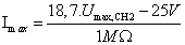

Figure 9: Dependence of cumulative probability of voltage maxima from channel 2 on the impact areas (pos1-7).

Figure 10: Dependence of cumulative probability of voltage maxima from channel 2 and surface currents on the impact areas 1-7.
The maximum current impulses are varying between 0,5 and 3 μA. Also the amplitudes depend on the plastic deformation of the piezoelectric surface of the impact area on the PZT-specimen, Figure 11. The surface deformation at the areas 2-6 has not a clear structure as it can be seen at areas 1 and 7. At the areas 1 and 7 local circular deformations of the surface are visible. These surface deformations lead to the conclusion that the tungsten pin has impact the specimen at the same position, whereas the contact point between the pin and the surface at position 2-6 varied. The variation of the local impact area plays an important role on the emission properties. Also the impact depth and the position have influence on the emissions. The impact depth of the surface at its deformation cause high dipole moment generation and high signal amplitudes. This is the reason for the high voltage and current amplitudes at area 1. The deformation degree of the surface of area 3 is lower than of area 2, this is reason for lower voltage amplitudes at area 3. The deformation degree and impact depth at area 7 is lower, than the deformation degree at other areas and the amplitudes are also lower. The experimentally determined voltage amplitudes at the oscilloscope channels 2-4 show a correlation with the estimated values by theoretical approach in Figure 2. The enhanced surface currents can be estimated by means of the shown relationship between surface currents and voltage amplitudes at equation 7-10 and the dependence of the elastic wave propagation, shown at equation 1-6. For description of the dependence of current flow on Lead Zirconium Titanate surfaces on dipole moment generation during mechanical impact, the influence of the degree of plastic deformation has to be taken as deformation factor k into account. On this way the surface current value can be described as
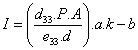
Where d33, P, A, e33, d describe the mentioned factors from equation 1-5 and equation 7, a and b are the factors from Equation 11 and the material factor, that vary from 0,1 and 0,3.

Figure 11: Dependence of maximum voltage amplitudes from channel 2 and surface currents on the impact areas 1-7.
The properties of bulk PZT ceramics were tested. It was shown that PZT material is able to generate current flow on its surface due to mechanical impact loading in μA - range. The enhancement of current flow on Lead Zirconium Titanate surfaces depends on dipole moment generation and the degree of surface deformation. Also a dependence on the position of impact area exists. Based on the obtained results it can be concluded that sensors, based on bulk PZT-ceramics are suitable for high efficient stress distribution analysis on the surface of machine components. The stress distribution can be acquired with high temporal and spatial resolution. One of the possible applications of such sensor systems is structural health monitoring.
This work was carried out within the framework of the German Federal Ministry of Education
Research Program ‘MEMS on MID’.