International Journal of Advanced Research in Electrical, Electronics and Instrumentation Engineering
ISSN ONLINE(2278-8875) PRINT (2320-3765)
ISSN ONLINE(2278-8875) PRINT (2320-3765)
Saritha Thomas Vaidyan1, Rabiya Rasheed2
|
| Related article at Pubmed, Scholar Google |
Visit for more related articles at International Journal of Advanced Research in Electrical, Electronics and Instrumentation Engineering
Here a soft-switching pulse width modulation (PWM) non-isolated bidirectional dc-dc (BDC) converter embedding an edge-resonant switched capacitor (ER-SWC) cell is presented. Bidirectional dc-dc converters serve the purpose of stepping up or stepping down the voltage level between its input and output. Bidirectional dc-dc converter has the capability of power flow in both the directions. The conceptual bidirectional dc-dc converter treated here can be operated in two modes: - buck mode (step-down) operation and boost mode (step-up) operation. The converter here operated in discontinuous conduction mode (DCM). So the converter can achieve high-frequency zero-current softswitching (ZCS) turn-on and zero-voltage soft-switching (ZVS) turn-off operations in the active switches. Those advantageous properties enable a wide range of soft-switching operations together with a high-voltage step-up conversion ratio with a reduced current stress. Circuit design guidelines based on the soft-switching range is introduced. Then, a theoretical analysis is carried out for investigating the step-up voltage conversion ratio. The simulation is carried out here in MATLAB/Simulink platform. For demonstrating the effectiveness of the softswitching PWM bidirectional dc-dc converter, a 22W-40kHz prototype is evaluated in experiments, and then its performances are discussed.
Keywords |
||||||||||||||||||
| Bidirectional dc-dc converters, soft-switching, Edge-resonant, Discontinuous Conduction | ||||||||||||||||||
INTRODUCTION |
||||||||||||||||||
| Bidirectional dc-dc converters (BDC) have recently received a lot of attention due to the increasing need to systems with the capability of bidirectional energy transfer between two dc buses. Apart from traditional application in dc motor drives, new applications of BDC include energy storage in renewable energy systems, fuel cell energy systems and uninterruptible power supplies (UPS). The fluctuation nature of most renewable energy resources, like wind and solar, makes them unsuitable for standalone operation as the sole source of power. A common solution to overcome this problem is to use an energy storage device besides the renewable energy resource to compensate for these fluctuations and maintain a smooth and continuous power flow to the load. As the most common and economical energy storage devices are batteries and super-capacitors. A dc-dc converter is always required to allow energy exchange between storage device and the rest of system. Such a converter must have bidirectional power flow capability with flexible control in all operating modes. To charge and discharge the storage element, the bidirectional DC-DC converter is used. Here a non-isolated bidirectional edge-resonant switched capacitor cell-assisted soft-switching dc-dc converter is presented. It is derived from an edge-resonant switched capacitor cell-assisted soft-switching PWM boost dc-dc converter [1]. The bidirectional converter can be operated in two modes: buck mode and boost mode. Edge resonance means resonance occurs at rising or falling edge of the PWM signal. The converter is operating in discontinuous conduction mode. By adopting discontinuous conduction mode (DCM) scheme, the conventional PWM boost dc-dc converter can attain the soft commutation naturally at the turn-on of the active switch and zero-current soft-switching (ZCS) turn-off of the freewheeling diode in the wide range of load variation without any additional circuit component. Those advantages lead to the simplicity in the main circuit configuration and the control systems. | ||||||||||||||||||
| However, there exists an inherent technical issue in the DCM scheme: the current stress in the power devices and components as well as in the input smoothing capacitor is larger than that of the PWM boost dc-dc converter in CCM. To overcoming the drawbacks of the PWM boost dc-dc converter in DCM, employment of the edge-resonant switched capacitor (ER-SWC) cell [13] is one of the effective techniques due to its high efficiency and high scalability characteristics. In the soft-switching PWM boost dc-dc converter with the ER-SWC cell, a wide range of soft-switching operations can be achieved under the condition of DCM/critical conduction mode (CRM) in the input dc current without any circulating current, while the current stresses in the power devices and the passive components can also be mitigated owing to the edge resonance within the switching cell. | ||||||||||||||||||
PROPOSED TOPOLOGY |
||||||||||||||||||
| The modified converter is a bidirectional edge-resonant switched capacitor cell-assisted soft-switching PWM dc-dc converter. The circuit configuration of the bidirectional ER-SWC soft-switching PWM dc-dc converter shown in Fig.1 | ||||||||||||||||||
| The ER-SWC cell consists of four active switches, , and &, two diodes ,a resonant capacitor Cr , and a resonant inductor . This converter can work in two modes of operation i.e. in buck mode or in boost mode. When the switches and are on, the converter act as a boost converter. At that time and & are off. In buck modeand &, are operated. During that time and are off. Edge resonance means resonance occurs at the rising or falling edge of the PWM signal. The modified converter is an edge-resonant soft-switching converter,that means softswitching happens at the rising or falling edge of the gate pulse | ||||||||||||||||||
OPERATION PRINCIPLE |
||||||||||||||||||
| A. Boost mode | ||||||||||||||||||
| In this mode the dc-dc converter acts as a boost converter. The gate pulse is given to and, keeping and & off. The mode transitions with the simplified equivalent circuits are shown in Fig.2. The circuit operation during one switching cycle is divided into five sub modes, as described in the following. | ||||||||||||||||||
| Mode 1 [ (,, ZCS turn-on mode): The inductor currentis zero, and the active switches ,and , are simultaneously turned ON atand the switch currents &rise gradually from the zero initial value with the edge resonance by and . Thereby, ZCS turn-on commutation can be achieved in and | ||||||||||||||||||
 |
||||||||||||||||||
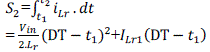
| Mode 2 , (inductive energy storing mode): The resonant capacitor is completely discharged at br /> then, the diodes are forward-biased. The beginning time; of this sub mode and its inductor current can be determined from (1) as | ||||||||||||||||||
| During this interval,rises linearly as expressed by | ||||||||||||||||||
| The inductor current | ||||||||||||||||||
| where + DT and D denotes the duty cycle of and as defined by | ||||||||||||||||||
| During this mode, is defined by | ||||||||||||||||||
| where as expressed by | ||||||||||||||||||
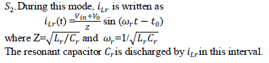
| This operation mode continues until the capacitor voltage ;t. | ||||||||||||||||||
| Mode 4 ], (inductor energy releasing mode): The resonant capacitor voltage rises up to the output voltage at ; then, the conduction interval of is terminated. The beginning time of the submode and the corresponding inductor current can be defined from (7) as | ||||||||||||||||||
| The inductor currentgradually decreases and naturally reaches to the zero level at . Accordingly, occurrence of the reverse recovering current in the output freewheeling diode can be mitigated. | ||||||||||||||||||
| Mode 5 (inductor current discontinuous Mode): Inductor current educes to zero level after ,which is determined from (11) by | ||||||||||||||||||
| The load current flows through the output capacitorin this submode; then, the inductor current keeps the zero level until the next switching cycle starts at . | ||||||||||||||||||
| B. Buck mode | ||||||||||||||||||
| In this mode the dc-dc converter acts as a buck converter. The gate pulse is given to and &, keeping S1 and S2 off. The gate pulse given to switch S4 is complimentary of S3. The mode transitions with the simplified equivalent circuits are shown in Fig.3 | ||||||||||||||||||
| Mode 1 [0 DT],(on,& off):During this interval is on, the ER-SWC cell is not conducting, because, and &are off and also are reverse biased. The input provides energy to the load as well as to the inductor. The voltage across the inductor can be represented as | ||||||||||||||||||
| Mode 2In this interval switch S3 is off. The inductor discharges through load. The inductor current flows through Lr-R0 -S2 -S1 | ||||||||||||||||||
ANALYSIS OF VOLTAGE CONVERSION RATIO |
||||||||||||||||||
| The analysis of the bi-directional converter is done by considering its boost mode operation[1]. The inductor current and voltage waveforms of the ER-SWC soft-switching PWM dc–dc converter in boost mode are illustrated and compared with those of the conventional hard-switching PWM boost dc–dc converter in DCM under the condition of the same duty cycle in Fig.4. The positive voltage–second area in fig.4 | ||||||||||||||||||
| As a result, the negative amplitude of in Fig. 5 is extended much more than that of the conventional type, then a larger output voltage i.e., higher voltage conversion ratio can be obtained in the ER-SWC dc–dc converter in boost mode. The voltage conversion ratio (M = Vo/Vin) of the ER-SWC boost dc–dc converter in DCM can be determined from the input and output power balance. By assuming the time origin to = 0 in Fig. 5 for simplicity, the time integrations of the inductor current in each submode are defined by | ||||||||||||||||||
 (16) (16) |
||||||||||||||||||
| Therefore, the average input current can be obtained by | ||||||||||||||||||
| Neglecting the power losses in the ER-SWC boost dc–dc converter, the power balances between the dc power source an be established as | ||||||||||||||||||
| The input power as | ||||||||||||||||||
| where Furthermore, deformation of (21) with (22) yields the equation regarding the voltage conversion ratio M as | ||||||||||||||||||
DESIGN GUIDELINE OF CIRCUIT PARAMETERS |
||||||||||||||||||
| The circuit parameters of and in the ER-SWC cell should be based on both of the maximum output power with the maximum duty cycle and the minimum output power Po,min with the minimum duty cycle Dmin. The determination of the zero crossing time of t4= DmaxT, the maximum output power Po,max can beexpressed as | ||||||||||||||||||
| Where represents the average current of at Po = Po,maxand this value can be obtained from (1), (4), (7), and (11); then, iLr,max means its maximum value. Then, the minimum output power Po,min can be given by | ||||||||||||||||||
| where Deformation of (25) yields the parameter of the resonant capacitor Cr as expressed by | ||||||||||||||||||
| The parameter of Lrshould meet the condition indicated asfollows | ||||||||||||||||||
SIMULATION RESULTS |
||||||||||||||||||
| The software used for simulation is MATLAB/Simulink.The proposed converter have two modes of operation, Boost Mode and Buck mode. In boost mode gate pulse is given to and . Fig.5 shows the simulink model of the bidirectional converter during boost mode. In boost mode the input voltage is in the range of 30V-100V and output is obtained as 200V. In buck mode gate pulse is given to and &. The gate pulse given to switch &. iscomplimentary of switch . Fig.6 shows the simulink model of the bidirectional converter during buck mode. In buck mode 200V is given as input and 30V is obtained as output. The switching frequency is 40 kHz. | ||||||||||||||||||
| Fig.7(a),(b) shows the input and output voltage waveforms during boost mode. Input voltage is30V and output voltage is obtained as 200V. | ||||||||||||||||||
| Fig.8 (a),(b) shows the waveforms of input and output voltage during buck mode. Input voltage is 200V andoutput voltage is obtained as 30V. | ||||||||||||||||||
| Fig.9 shows the hardware implementation of the Bidirectional DC-DC converter | ||||||||||||||||||
CONCLUSION |
||||||||||||||||||
| The Bi-Directional converter plays an important role in renewable energy applications. The proposed non-isolated bidirectional edge resonant switched capacitor cell assisted soft switching DC-DC converter can work in either boost mode or buck mode. This converter can achieve high-frequency zero-current soft-switching turn-on and zero-voltage soft-switching turn-off operations in the active switches. As a result a wide range of soft-switching operations together with a high-voltage step-up conversion ratio with a reduced current stress. | ||||||||||||||||||
ACKNOWLEDGMENT |
||||||||||||||||||
| Initially, I would like to thank, the God Almighty for showing his blessings on me for successful completion of this work. Also I would like to thanks teachers, friends and parents. | ||||||||||||||||||
Figures at a glance |
||||||||||||||||||
|
||||||||||||||||||
References |
||||||||||||||||||
|


