International Journal of Advanced Research in Electrical, Electronics and Instrumentation Engineering
ISSN ONLINE(2278-8875) PRINT (2320-3765)
ISSN ONLINE(2278-8875) PRINT (2320-3765)
J. Jenifa1, C.Jacob Ebbipeni2, V.Monisha3
|
| Related article at Pubmed, Scholar Google |
Visit for more related articles at International Journal of Advanced Research in Electrical, Electronics and Instrumentation Engineering
In all type of electronic circuits, reducing the energy dissipation is one of the major topics of interest. In bus interconnect lines, the dynamic power dissipation contributes a significant fraction in the overall power dissipation. Hence, the main objective of VLSI designers is to minimize the power dissipation, switching activity, on the interconnect lines. A modified Embedded Transition Coding Scheme reduces the number of bus lines in conventional parallel-line bus by multiplexing each m-bits onto a single line is proposed. The advantage of Serial Line Bus is that they have fewer lines, reducing crosstalk and area. Serializing parallel buses tends to increase bit transition and power dissipation. The proposed Embedded Transition Inversion Coding method uses an efficient encoding and decoding technique in order to minimize the transition activity and power consumption in serial links. In previous method a transition indication bit is added in every data word to represent a inversion indication. This extra bit increases the number of transmitted bits, number of bit transitions and power dissipation. This proposed coding scheme is used to solve the issue of the extra indication bit. This scheme eliminates the need of sending an extra bit by embedding the inversion information in the phase difference between the clock and the encoded data.In this proposed method Alexander Phase Detector is replaced by Half Rate Phase Detector. The proposed system is simulated by using Xilinx 13.1 software to get efficient output. The proposed system result analysis shows better than the existing method.
Keywords |
||||||||||||||||
| Serial Interconnection, Embedded Transition Inversion (ETI) coding, Phase Encoder, Phase Detector, Bit two inverter. | ||||||||||||||||
LITERATURE SURVEY |
||||||||||||||||
| Parallel buses multiplexed into a serial link enables an improvement in terms of reducing interconnect area, coupling capacitance, and crosstalk [1], but it increases the overall switching activity factor (AF) and energy dissipation. Therefore, an efficient coding method needed to reduce the switching AF is an important issue in serial interconnect design. Existing methods solves the problem of increased switching activity for the parallel buses. A bus-invert method [2] minimizes the switching activity for the parallel buses. This method transmits the original or inverted data to minimize power dissipation and switching activity. Improved bus-invert coding methods such as the partial bus-invert coding [3] and weight-based bus invert coding methods[4]reduces power dissipation. But it uses extra control bit to send the inversion indication signal. It increases extra transmission line. Extra channel problem is solved by the serial coding technique[5]. In this method an extra information bits are added to the back of the original data word. It solves the area overhead problem. But it increases data latency. To reduce power dissipation Joint crosstalk avoidance code and error correction code[7] are proposed. Combining serializing bus with the error correction code joint crosstalk avoidance code[8] is proposed to reduce the power. Transition inversion coding (TIC) [9] technique reduces switching activity for random data and to detect errors. An extra transition indication bit is added in every data word. This extra bit not only increases the number of transmitted bits, but also increases the transitions and latency. | ||||||||||||||||
INTRODUCTION |
||||||||||||||||
| Power dissipation is a major critical design criterion in most system designs, especially in portable battery-driven applications. With the increasing drive towards System On Chip (SOC) applications, power has become an important parameter that needs to be optimized along with speed and area. The main sources of power dissipation in VLSI circuits are the leakage currents, the stand-by current, the short-circuit current, and the capacitance current (due to charging and discharging of node capacitances during transitions).The major source of power dissipation is given by, | ||||||||||||||||
| where,P is the capacitive power dissipation | ||||||||||||||||
| CL is capacitance at the output of the node | ||||||||||||||||
| Vddis the supply voltage | ||||||||||||||||
| fclkis the clock frequency | ||||||||||||||||
| E(sw) is the average number of output transitions | ||||||||||||||||
| Serialization reduces the number of wires and leads to a larger interconnect width and spacing. A large interconnect spacing reduces the coupling capacitance, while the wider interconnects reduce the resistivity. A significant improvement in the interconnect energy dissipation is achieved by applying different coding schemes and their proposed multiplexing techniques. However, the power reduction decreases when the degree of multiplexing increases. The Modified Embedded Transition Inversion (ETI) Coding scheme solves the issue of the extra indication bit. This scheme eliminates the need of sending an extra bit by embedding the inversion information in the phase difference between the clock and the encoded data. When there is an inversion in the data word, a phase difference is generated between the clock and data. Otherwise, the data word remains unchanged and there is no phase difference between the clock and the data. The receiver side adopts a phase detector (PD) to detect whether the received data word has been encoded or not. Simulation results shows that the proposed coding scheme has low transitions for different kinds of data patterns. | ||||||||||||||||
EFFICIENT COMMUNICATION |
||||||||||||||||
| The architecture of the Modified ETI Encoding and the Decoding Scheme is shown in Fig. 5. | ||||||||||||||||
A. ETI Encoder |
||||||||||||||||
| The ETI encoder includes the check transitions block, buffer, B2INV, and phase encoder. The check transition block is shown in Fig. 6. In the ETI encoder part, the input data are stored in the buffer and wait for the check transition operation is completed. The number of transition and threshold value in a data word are used to set the decision bit. The decision bit is used to control the encoding process in the inverter and the phase encoder block. | ||||||||||||||||
| The check transition circuit counts the transition in the data word. A transition between two bits is calculated by performing the XOR between them. D-FF stores the previous bit, the XOR operation is performed between the previous bit and the present bit. The WL indicator block counts the length of the data word. It generates a high signal at the first bit of the data word to reset the adder and the D-flip-flop. The number of transition in a data word is counted in the adder and sets the decision bit to high when the Nt≥ Nth. If the decision bit is set to 1 the input data becomes inverted. The decision bit is used to control the encoding process in the inverter and the phase encoder block. When the decision bit is zero, the inverter passes the non-inverted bit stream. Otherwise, the bit stream is encoded. | ||||||||||||||||
| The inversion encoding operation can be expressed as | ||||||||||||||||
 |
||||||||||||||||
| The inverter block is shown in the Fig.7 | ||||||||||||||||
| The phase generator is used to generate phase difference between the encoded data and the clock. Depending on the encoded data, there are three types of phase encoding: the one cycle delay, the half cycle delay and the special data word. The phase encoder is shown in the Fig. 8. | ||||||||||||||||
B. ETI Decoder |
||||||||||||||||
| The ETI encoder generates the phase difference between the clock and the data word. A PD identifies an early or delayed phase. Modified ETI Coding scheme adopts the Hogge Phase Detector [13]. The PD is shown in Fig. 9. | ||||||||||||||||
| The PD is controlled by the clock CK and input data Din. PDs for random data must provide two essential functions. Data transition detection and Phase difference detection occurs when the clock CK and input data Din are valid, the PD is activated to identify the phase relation between the clock and the data. The PD can determine whether a data transition exists from the condition that the clock leads or lags the data. The decision bit is used in the inverter for the decoding. The decoding operator in the inverter is the same as that in the encoder. The phase detector identifies whether the encoded data from the encoder block is encoded data or unencoded data depending on the decision bit. | ||||||||||||||||
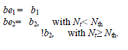
| The inversion decoding operation for the decoded output bd1bd2 is | ||||||||||||||||
| bd1= be1 bd2 = be2, with Nt< Nth !be2, with Nt≥ Nth . |
||||||||||||||||
| If the decision bit is set to zero the data from the encoder block is unencoded data. if the decision bit is set to one the data from the encoder block is the encoded data. After decoding operation the datas are parallized in the deserializer. | ||||||||||||||||
SIMULATION RESULTS AND DISCUSSION |
||||||||||||||||
| The snapshot shown in figure is taken from the modelsim 6.a software which shows the 8-bit data encoding and decoding using Modified ETI Algorithms for the input data’s 1111000 and 10101010 respectively. | ||||||||||||||||
| For the input data 1111000 as shown in the Fig 9 the number of transition is 1 (Nt=1). The threshold value is set as half the bus word length (Nth=4). Here the number of transition is l less than the threshold value 4. Hence there is no need for encoding the input data. The original data is sent as it is. | ||||||||||||||||
| For the input data 10101010 as shown in the Fig 10 the number of transition is 1 (Nt=7). The threshold value is set as half the bus word length (Nth=4). Here the number of transition is 7 greater than the threshold value 4. Hence the input data need to be encoded to reduce the switching activity. So the original data is inverted and then phase encoded in the encoder block and then it is transmitted to the channel. At the receiver block the encoded input data is phase decoded and inverted to get the original output value. | ||||||||||||||||
| Register Transfer Logic (RTL) representation of the Modified ETI scheme is shown in the Fig 11. | ||||||||||||||||
COMPARATIVE ANALYSIS |
||||||||||||||||
| Comparative analysis of ETI encoding and decoding Scheme and Modified ETI encoding decoding scheme can be done by the device utilization summary extracted from Xilinx. Device utilization summary is the report of used device hardware in the implementation of the chip such as RAM, ROM, slices, flip flops etc. Synthesis report shows the complete details of device utilization as total memory utilization. The device targeted for synthesis on SPARTEN-3 FPGA . Table 1 compares the hardware utilization for ETI encoder decoder and the Modified Encoder decoder scheme. Selected Device: 3s100etq144-4 | ||||||||||||||||
CONCLUSION |
||||||||||||||||
| Existing ETI coding and the Modified ETI coding is implemented in Xilinx 13.1 and functionally checked in Modelsim 6.a software. A comparative analysis is done with respect to hardware utilization. This scheme eliminates the need of sending an extra bit by embedding the inversion information in the phase difference between the clock and the encoded data thereby reducing the extra bit transition and switching activity. The proposed Modified ETI Coding scheme is reduces the switching activity and power compare with the existing ETI scheme. The proposed technique is suitable for most of the Low Power VLSI applications. | ||||||||||||||||
Tables at a glance |
||||||||||||||||
|
||||||||||||||||
Figures at a glance |
||||||||||||||||
|
||||||||||||||||
References |
||||||||||||||||
|


