International Journal of Advanced Research in Electrical, Electronics and Instrumentation Engineering
ISSN ONLINE(2278-8875) PRINT (2320-3765)
ISSN ONLINE(2278-8875) PRINT (2320-3765)
B.Pradeep, V.Vishnu Vardhan
|
| Related article at Pubmed, Scholar Google |
Visit for more related articles at International Journal of Advanced Research in Electrical, Electronics and Instrumentation Engineering
Reversible Logic is an emerging technology; it has hellocious applications in various fields. Reversible logic implementation reduces loss of entropy because of bit manipulations. Conservative reversible logic gate obeys reversible logic rules and also satisfies the property that there is equal number of 1s in the outputs as in the inputs. In this work, modified design of SCRL (Super Conservative Reversible Logic) gate for the design of reversible quantum circuit is presented. The proposed SCRL Integrated Qubit gate has 1 control input which swaps n-1 depending on control input. Barrel shifter forms an integral component of many computing systems. As an example of using the proposed SCRL gate to design efficient reversible quantum circuits, the design of reversible barrel shifter with zero ancilla inputs and zero garbage outputs is illustrated.
I. INTRODUCTION |
| Reversible Logic is an emerging technology; it has hellocious applications in various fields, such as Nano computing, DNA Computing QCA (Quantum Cellular Automata),Optical Computing etc.., Limitations of CMOS in Deep sub Micron Regime Leads to failure of Moore’s law, leads to development of Reversible circuits. These are more immune to Information loss, this Information loss is in the form of energy dissipated for every bit change. Reversibility concept is an idea from Launder[2] , there is a minimum amount of energy required to change one bit of information, known as the Landauer’s limit kT ln2 (0.69315).At25 °C, energy loss for one bit change is 0.0178 ev.Bennett [3]showed that loss is negligible if we implement reversible logic. So the primary goal of reversible computing is to minimize energy loss in computing devices and promote speed and density. We present VHDL representation for proposed design .In section II we represents Basic terminology of reversible logic and basic gates in Reversible logic .In section III we represent Proposed Work using Prior Work ,In section V conclusion . |
II. TERMINOLOGY AND GATES |
| The multiple output Boolean function G(x1; x2;:::; xn) of n Boolean variables is called reversible if the number of inputs is equal to the number of outputs ,any output pattern has an only one input representation. |
| Basic Gates in reversible logic |
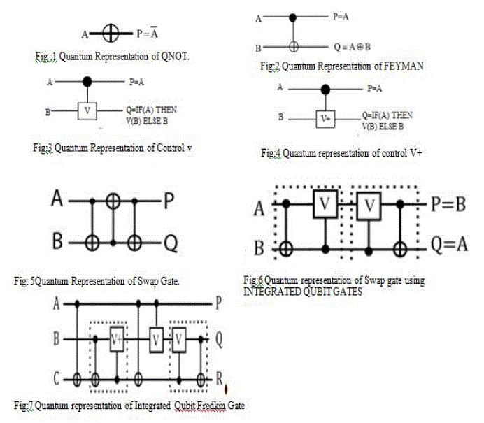
| The reversible gates used in this work are the NOT gate, the CNOT gate, the Toffoli gate and the Peres gate. Each reversible gate has the quantum cost and the delay associated with it. The NOT gate and the CNOT gate have the quantum cost of 1 and delay of 1 Δ; Control V control V + are the basic gates ,by using these gates many gates using reversible logic were designed to meet the requirement , |
| A)FEYMAN GATE:. |
| This gate uses one CNOT Gate with quantum cost 1, Details of CNOT gate and Quantum Representation in fig 2 |
| B)Control V and Control V+: |
| The controlled-V gate is shown in Fig. 3 In thecontrolled-V gate, when the control input l A=0 then thequbit B will pass through the controlled part unchanged, i.e., Q=B. When A=1 then the unitary operation V =is applied to the input B, i.e., Q=V(B). |
| Thecontrolled-V + gate is shown in Fig4. In the controlled-V + gate when the control input |
| l A =0 then the qubit B willpass through the controlled part unchanged, i.e., we will haveQ=B. When A=1 then the unitary operation V + = V −1 isapplied to the input B, i.e., Q=V +(B). |
| C)Integrates Qubit Gates: |
| These are two bit quantum gates allows minimized construction of locally reversible logic structures.[2]. |
| D)Fredkin Gate using IQ Gates[FG]: |
| By using IQ Representation for Fredkin Gate Reduces quantum cost to 5.Quantum Representation of Fredkin gate is in Fig7 |
| E)Swap Gate: |
| Reduced implementation of the reversible Swap Gate[2], which is designed using two integrated qubit gates, and produces a swap of the two input values on the output gate. Previously, the swap gate was implemented using three Feynman gates which produced the outputs (P=A⊕(A⊕B) and Q=A⊕(A⊕B)⊕(A⊕B)which produces the swap, and incurred a quantum cost and delay of 3.The proposed implementation is accomplished with a quantum cost and delay of 2, was verified using VHDL, and is shown in Figure 5 and 6. |
 |
III. LITERATURE SURVEY |
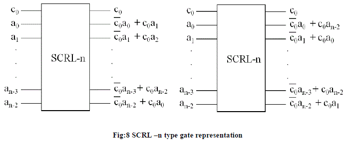
| In this work, we have proposed a new n × n (n inputs and noutputs) conservative reversible logic gate named SCRL gate. In theSCRL gate, out of n inputs there is 1 control input and n −1 datainputs. Let us define n inputs of the SCRL gate as c0; a0; a1:::an-2where c0 is the control input and a0 to an-2 are the data inputs. Theoutput function of the SCRL gate is defined as follows: |
| The control input c0 is hardwired to the first output of the SCRLgate |
| The remaining n − 1 outputs have the output function c0ai +c0ak, where ai is the ith input and i ∈ {0 to n −2}; and ak is the kth input where k ∈ {0 to n − 2} such that k = i and ak cannot occur as the coefficient of c0 in any other output function. |
| Two examples of n × n SCRL gate are shown in Figure 8. FromFigures 8(a) and8(b) it can be observed that there can be more than one n × n SCRL gates depending on the selection of the coefficient of c0 in the output function: c0ai + c0ak. |
 |
| A)SCRL gate as a Super Set of Fredkin gate[1]: |
| A 3x3 SCRL gate (SCRL-3) is similar to the existing Fredkin gate. Theexisting Fredkin gate is very limited in functionality as compared to the proposed generalized SCRL gate as illustrated below |
| The existing Fredkin gate is not suitable for designing SCRL gates with even inputs, It can be observed that SCRL-4 gatecannot be designed from the existing Fredkin gate. |
| The odd inputs SCRL gates such as SCRL-5, SCRL-7, etc. can be defined as SCRL-(2n+1) where n is an integer such that n≥1. By cascading the Fredkin gates in series, we can design odd inputs/outputs equivalent of SCRL gates. |
| The Fredkin gate based logical block can do the pair wise bit swap but it is not capable of performing the swap of any two input bits. Our proposed SCRL gate has overcome this limitation as it is more generic in nature and can swap any two input bits when control input is 1. |
| IV. PROPOSED SCRL INTGRATED QUBIT GATE |
| In SCRL we can do pair wise swapping of bits but also it can swap two or more bits depending on control inputs like SCRL gate [1], InSCRL [1] uses swap gate as shown in Fig 5 with qubit gate its quantum cost is ‘3’ unit .Proposed INTEGRATED QUBIT based SCRL uses swap with which uses integrated qubit gates as shown in fig 6 .The cost reduces from ‘3’ to ‘2’ for 1 swap gate. |
| A)PROPOSED DESIGN OF A REVERSIBLE BARREL SHIFTERUSING SCRL GATE |
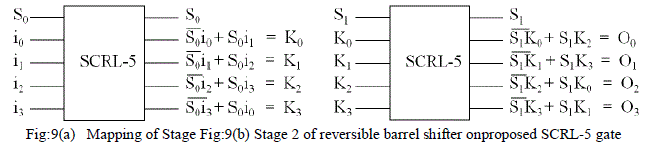
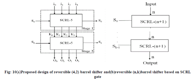
| For a (n,k) reversible barrel shifter the input data is represented as in-1; in-2; in-3; ::::; i2; i1; i0. The (n,k) reversible barrel shifter has log2(n) stages. The log2(n) number of stages of a(n,k) reversible logical right shifter is controlled by control signalsSk-1,Sk-2,....,S1,S0. The S0will work as the control signal for 1ststage, S1 will work as the control signal for 2nd stage and so on. Thus for mth stage the control signal will be Sm-1 where m= 1 tok-1. We can observe that each stage of the (n,k) barrel shifter can beimplemented using SCRL-(n+1) gate. It is to be noted that for the(i+1)th stage of (n,k) reversible barrel shifter where i=0 to k-1, Siwill be the control signal of the SCRL-(n+1) gate.The proposed design of (n,k) reversible barrel shifter using SCRL with integrated qubit gates is illustrated with an example of (4,2) reversible barrel shifter.Figure 9 shows the equations of (4,2) reversible barrel shifter generatedusing SCRL gates, the stage 1 of the reversible barrel shiftergenerates the intermediate outputs K0 to K3. In stage 2 the finaloutputs are generated as O0 to O3. Thus, the proposed SCRL-5 gate implements the stage 1 with Zero ancilla inputs and zero garbage outputs. The Stage 2 of (4,2)reversible barrel shifter generates the final outputs O0 to O3 as shownin Table1 that can be mapped to another SCRL-5 gate as illustrated in Figure 9(b). |
 |
| The complete design of the proposed (4,2) reversiblebarrel shifter cascading Stage 1 and Stage 2 with two SCRL gates isshown in Figure 10(a). Thus, using the proposed design methodologyof (4,2) reversible barrel shifter, the (n,k) reversible barrel shiftercan be designed using SCRL gates as illustrated in Figure 10(b)where each stage is implemented with proposed SCRL-(n+1) gate. |
| The proposed (n,k) reversible barrel shifter based on SCRL gates canbe summarized as : Cost reduced by 1 unit for 1 swap gate Number of SCRL Gates (NSCRL) = k Number of Garbage Outputs (NGO) = 0 Number of Ancilla Inputs (NAI) = 0 |
 |
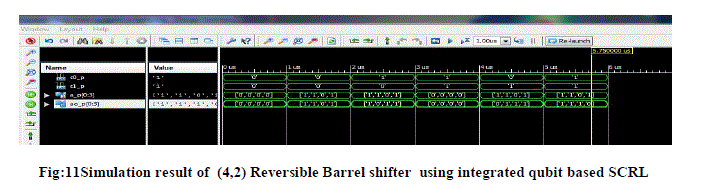
| B)Simulation Result for (4,2) Barrel Shifter: |
 |
V. DISCUSSIONS AND CONCLUSIONS |
| We present a novel conservative reversible logic gate (SCRL gate)which is superior, and is a superclass of Fredkin gate. Further, the design of (4,2) reversible barrel shifter with zero ancilla inputs andzero garbage outputs is presented based on the proposed SCRL gate.We conclude that the use of the specific reversible gate for a particularcombinational function can be very much beneficial in minimizing thenumber of ancilla inputs and garbage outputs in reversible quantumcircuits. All the proposed reversible designs are functionally verified at the logical level by using the VHDL and the HDL simulators. In future work, we would like to illustrate the various other applications of the proposed SCRL gate in the design of reversible quantum circuits. |
References |
|