International Journal of Advanced Research in Electrical, Electronics and Instrumentation Engineering
ISSN ONLINE(2278-8875) PRINT (2320-3765)
ISSN ONLINE(2278-8875) PRINT (2320-3765)
Bhuvaneswaran.M1, Elamathi.K1
|
| Related article at Pubmed, Scholar Google |
Visit for more related articles at International Journal of Advanced Research in Electrical, Electronics and Instrumentation Engineering
Minimizing area and power is the more challenging task in modern VLSI design. Adders are the most widely used components in many circuits, the design of area and power efficient high-speed data path logic systems forms the largest areas of research in VLSI system design. The study presents a new dynamic logic named sp-D3L that overcomes the speed limitations of D3L. Power consumption is significantly reduced by using the sp-D3L logic. CSLA is one of the fastest adders used in many data-processing processors to perform fast arithmetic functions. From the structure of the CSLA, it is clear that there is span for reducing the area and power consumption in the CSLA.
Keywords |
| Adder, Carry select Adder, Performance, Low power, Simulation |
I. INTRODUCTION |
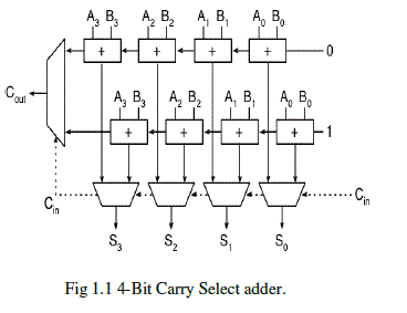
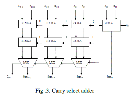
| Design of area- and power-efficient high-speed data path logic systems are one of the most substantial areas of research in VLSI system design. In digital adders, the speed of addition is limited by the time required to propagate a carry through the adder. The sum for each bit position in an elementary adder is generated sequentially only after the previous bit position has been summed and a carry propagated into the next position. The CSLA is used in many computational systems to alleviate the problem of carry propagation delay by independently generating multiple carries and then select a carry to generate the sum. However, the CSLA is not area efficient because it uses multiple pairs of Ripple Carry Adders (RCA) to generate partial sum and carry by considering carry input Cin and Cout then the final sum and carry are selected by the multiplexers (mux). |
| The performance of a full adder circuit depends to a great extent on the type of design style used for implementation as well as the logic function realized using the particular design style. For instance, a standard CMOS implementation allows circuits to achieve a reasonable power delay product with high noise margins, regular layout and relatively higher tolerance to process variations.Dynamic implementations on the other hand may yield an extremely fast design but end up paying higher costs in the overall power consumption. Data driven dynamic logic(D3L) and Split pre-charge data driven dynamic logic(sp-D3L) are two design styles which allow high performance dynamic circuit design without the additional power consumption in the clock distribution network. Thus these styles form interesting implementation strategies for realizing high performance, power-efficient full adders. Power consumption is one of the critical design factors in modern VLSI design. |
| A carry-select adder takes the two input bits A and B and creates a true and partial sum from them. These go into a multiplexer which chooses the correct output based on the actual carry in. Carry-select adders are made by linking 2 adders together, one being fed a constant 0-carry, the other a constant 1-carry. Most Minecraftian carry-select adders are not true carry-select adders, but simulate the operation of a carry-select in Mine craft. |
 |
II. PERFORMANCE CHARACTERIZATION AND COMPARISION |
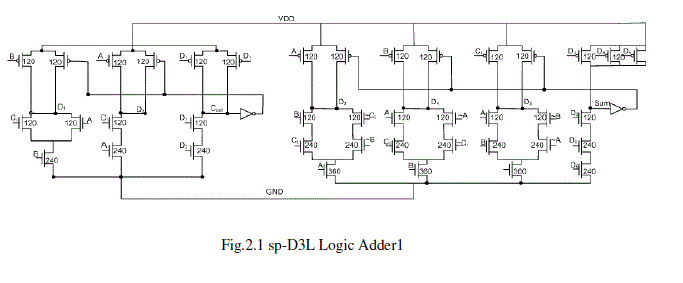
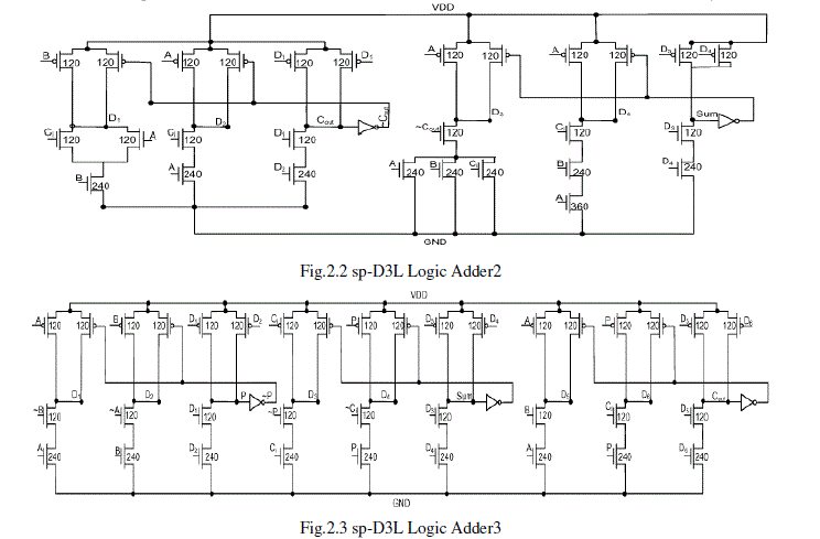
| The performance of a full adder circuit depends to a great extent on the type of design style used for implementation as well as the logic function realized using the particular design style. For instance, a standard CMOS implementation allows circuits to achieve a reasonable power delay product with high noise margins, regular layout and relatively higher tolerance to process variations. Dynamic implementations on the other hand may yield an extremely fast design but end up paying higher costs in the overall power consumption. D3L and sp-D3L are two design styles which allow high performance dynamic circuit design without the additional power consumption in the clock distribution network. Thus these styles form interesting implementation strategies for realizing high performance, power-efficient full adders. Fig. 1 shows three full adder implementations in the recently proposed sp-D3L design style. Along with the choice of logic function and implementation style, the sizing of the transistors also plays an extremely important role in the optimization of circuit performance, power consumption, noise margins, fan-in, fan-out, etc. For dynamic adders it was observed that progressively sizing the rest of the transistors yielded the best power-delay Product while also maintaining drivability of the adder circuits. For the interested reader, we have described the results of various sizing methodologies on the standard static, domino and D3L adders and 16-bit carry select adder. It was observed that progressive sizing of transistors yielded the best performance of the power for each of the adder circuits considered. As a result, all our adders were sized accordingly. For the pass-transistor and transmission gate based adders i.e. adders without drivability, we kept minimum sizes on all the transistors. This was found to be the best option since any performance advantage gained by upsizing the pMOS transistors in these circuits is off-set by the increase in power. While the speed advantage itself is off-set due to the inevitable use of buffers at the outputs of these adders. Hence, minimum sizing all the transistors yielded the best power-performance and area trade off. |
 |
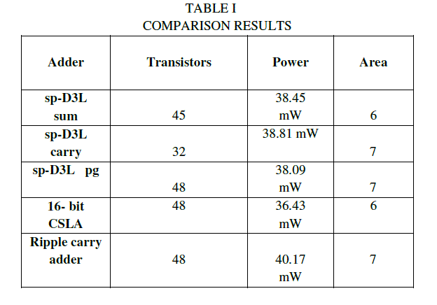
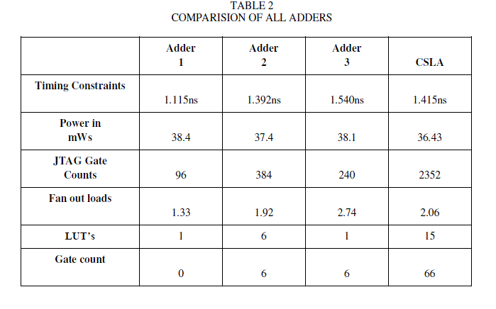
| The table 1 reports the average power consumption when executing the set of all possible input combinations to the adders. The full adder functions characterized using the sp-D3L methodology provide the lowest power depends upon the transistor with the sp-D3L adder working almost twice as fast as the standard adders selected in the study. |
 |
| The drawback of the existing adders is of course the high power consumption, due to the large number of transistors as well as the multiple paths to ground present in the sp-D3L implementations. With respect to the choice of logic function to implement, the full adder was observed to perform the best when implemented using the PROPAGATE and GENERATE signals. This can be attributed to the fact that this function allows for smaller number of transistors stacked in series and shows the lowest capacitance at the output node. This shows that the capacitance at the output node forms the most critical component of the adder speed irrespective of the number of stages of circuits before getting the SUM and CARRY outputs. |
| Power consumption in CMOS circuits has always been one of the primary concerns of the designer especially when designing for applications with strict power constraints. To facilitate the ideal choice of adder topology for scaled voltage or power-constrained applications, it is necessary to analyze adder performance with scaled supply voltages. It can be observed that the sp-D3L adder shows a consistent improvement in power delay system when supply voltage is scaled in contrast to all the other adders whose performance characteristics worsen as the supply voltage is scaled down. Under scaled voltage, the mirror adder and the adders show the worst power delay product profiles implying that they are unsuitable for operation under scaled supply voltages. It can also be seen that the performance of the TG adder is significantly worse at lower than nominal supply voltages whereas the pass transistor Multiplexer based adder completely failed when operated below 0.9 V. Thus it is clear that transmission gate and pass transistor-based adders cannot be used in extremely scaled operating voltage scenarios. |
III. RELATED WORK |
| Jiang, Sheraidah, Wang, and J. Chung,(2004) has proposed that the 1-bit full adder is one of the most critical components of a processor, as it is used in the arithmetic logic unit, the floating-point unit, and address generation for cache or memory accesses. A variety of full adders using static and dynamic logic styles are available. The static energy recovery full adder requires only 10 transistors to implement a full adder. Intensive HSPICE simulation shows that the new adder has more than 26% in power savings over conventional 28-transistor CMOS adder. |
| Frustaci, Lanuzza, Zicari, Perri and Corsonellohas proposed that the data-driven dynamic logic is very efficient when low-power constraints. Differently from conventional dynamic domino logic, which exploits a clock signal, D3L uses a subset of the input data signals for pre-charging the dynamic node, thus avoiding the clock distribution network. Power consumption is significantly reduced, but the pre-charge propagation path delay affects the speed performances and limits the improvements. This study presents a new dynamic logic named split-path D3L that overcomes the speed limitations of D3L. When applied to a 16 _ 16 bit Booth multiplier realized with ST Microelectronics 65 nm 1V CMOS technology, the proposed technique leads to an EDP 25 and 30% lower than standard dynamic domino logic and conventional D3L logics. |
| SohanPurohit and Martin Margalahas proposed the sp-D3L adder for sum, carry and propagate and generate. There are 12 full adder circuits in the IBM 90-nm process. These include three new full adder circuits using the recently proposed split-path data driven dynamic logic. Based on the logic function realized, the adders were characterized for performance and power consumption when operated under various supply voltages and fan-out loads. |
IV.OUR CONTRIBUTION |
| Our project will implement the carry select adder instead of using full adder. There are different logic adders are introduced .In each adders we calculate the power and areas. Two 4-bit ripple carry adders are multiplexed together, where the resulting carry and sum bits are selected by the carry-in. Since one ripple carry adder assumes a carry-in of 0, and the other assumes a carry-in of 1, The carry out of each 4-bit block is connected to the carry in of the next 4-bit block. When combined in this manner, 16-bit signed binary numbers can be computed. Subtraction is accomplished using two's complement binary arithmetic. |
 |
 |
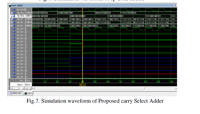
V. SIMULATION OUTPUTS |
 |
 |
 |
 |
 |
VI. CONCLUSION |
| The new split-path implementation of the full adder function was found to be a strong contender in terms of both performance-power efficiency as well as strong drivability. These adders are faster than ripple carry adders but slower than carry select adders. All the adders are designed using VHDL (Very High Speed Integration Hardware Description Language), Xilinx Project Navigator 9.1i is used as a synthesis tool and ModelSim XE III 6.2i for simulation. Wherever there is need of smaller area and low power consumption, while some increase in delay is tolerated, such designs can be used. These adders are faster than RCA. |
ACKNOWLEDGMENT |
| The authors would like to express their gratitude to Department of Electronics and communication Engineering,Muthayammal Engineering college, providing the valuable guidance and support to make it possible to experiment it practically. |
References |
|