International Journal of Advanced Research in Electrical, Electronics and Instrumentation Engineering
ISSN ONLINE(2278-8875) PRINT (2320-3765)
ISSN ONLINE(2278-8875) PRINT (2320-3765)
Mr R.G.Shriwastava1, Dr. M.B.Diagavane2, Dr. S.R.Vaishnav3
|
| Related article at Pubmed, Scholar Google |
Visit for more related articles at International Journal of Advanced Research in Electrical, Electronics and Instrumentation Engineering
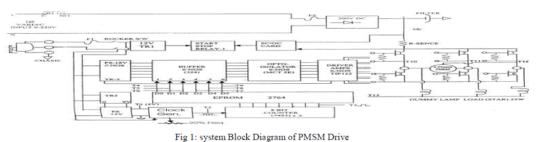
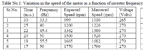
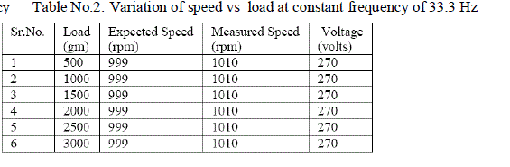
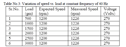
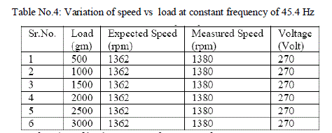
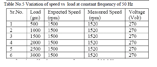
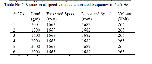
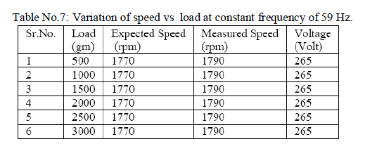
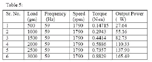
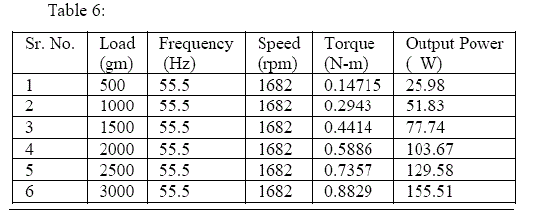
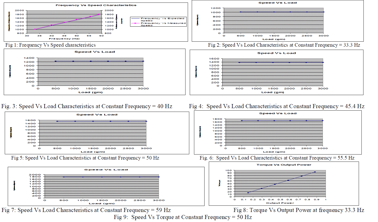
This paper describes the design and testing of PMSM drive for Automotive Industry. The impact of various circuits is discussed in detail. Permanent magnet synchronous motor is used here with three stator windings for the motor operation. Three supply voltage are obtained with the help of three phase MOSFET bridge inverters. MOSFET bridges are fed with fixed dc voltage which is obtained by rectifying ac voltage available from ac mains with the help of diode bridge. Shunt capacitor filter is used for filtering purpose. Operation of the MOSFET bridge is controlled by the control circuit. Gating pulses required to turn the MOSFET On are obtained from the control circuit. By controlling the frequency of the gating pulses frequency of the output from MOSFET bridge is controlled. Control circuit consists of clock generator counter and EPROM. First data required to generate gating pulses is calculated and is stored in EPROM. This data is outputted at the output of the EPROM by generating the address of the memory location with the help of 4 bit binary ripple counter. Clock input required for the operation of the counter is generated using IC 555 in astable mode. Frequency of the gating signals coming out of EPROM is dependent on the frequency with which addressing is done which is turn dependent on the clock frequency. Thus by varying the clock frequency of gating signal is varied. If frequency of gating signal is varied, then the MOSFET bridge output frequency is also varied. Thus we obtain variable frequency output. Gating signal outputted by EPROM cannot be directly applied to MOSFET bridge as they are very weak. So isolator and driver circuit is used. Necessary isolation of low power control circuit from high power bridge circuit is obtained by using opt isolator. The Experiment results show that by varying the inverter frequency the speed of the motor also gets varied. If the frequency increases the speed of the motor also increases and if the frequency decreases the speed of the motor also decreases. If the frequency is kept constant at particular value, the speed of the motor also remains constant, irrespective of the load.
Keywords |
| Permanent magnet synchronous machine. Permanent magnet material, MOEFET Inverter Circuit, clock signal generator, address generator, EPROM, Electric power Steering. |
I. INTRODUCTION |
| Permanent magnet synchronous motors (PMSM) are widely used in high-performance drives such as industrial robots and machine tools for their advantages on high power density, high-torque, free maintenance and so on. In recent years, the magnetic and thermal capabilities of the PM have been considerably increased by employing the high-coercive PM materials [1]. In last few years, permanent magnet synchronous motor (PMSM) consequently is acquired in more and more far-ranging application, because of its properties such as small volume, light weight, high efficiency, small inertia, rotor without heat problem, etc. [2]. Space vector pulse width modulation DTC is a technique to reduce the ripples of the electromagnetic torque and flux linkage. Direct Torque Control (DTC) is a new control method after vector control. It abandons decoupling thought of vector control, and uses the stator flux linkage directly to control the flux linkage and the torque of motor. Thus, the dynamic response of the System is very fast [3]. The DTC control strategy is applied for PMSM in order to improve the torque characteristics of the motor, which currently has caused the extensive attention of people. The traditional DTC usually adopts bang-bang control strategy to implement. But this control strategy cannot meet the system requirements both of torque and flux linkage at the same time, which leads to large fluctuations of flux linkage and torque generated by system and leads to the problem of pulse current and switches noise caused by higher switching frequency changes. The electrical machine that converts electrical energy into mechanical energy, and vice versa, is the workhorse in a drive system. Drive systems are widely used in applications such as fibers spinning mills, rolling mills, MAGLEV - linear synchronous motor propulsion, aircraft engines, paper and textile mills, electric vehicle and subway transportation, home appliances, wind generation systems, servos and robotics, computer peripherals, steel and cement mills, ship propulsion, etc. A machine is a complex structure electrically, mechanically, and thermally. Although machines were introduced more than one hundred years ago, the research and development (R&D) in this area appears to be neverending. However, the evolution of machines has been slow compared to that of power semiconductor devices and power electronic converters. An engineer designing a high-performance drive system must have the knowledge about machine performance, the dynamic model, and parameter variations. Industrial drive applications are generally classified into constant-speed and variable-speed drives. Traditionally, ac machines with a constant frequency sinusoidal power supply have been used in constant-speed applications, whereas dc machines were preferred for variable-speed drives. Dc machines have the disadvantages of higher cost, higher rotor inertia, and maintenance problems with commutator and brushes. Commutator and brushes, in addition, limit the machine speed and peak current, cause EMI problems, and do not permit a machine to operate in dirty and explosive environments. However, dc machine drive converters and controls are simple, and the machine torque response is very fast. |
II. PMSM DRIVE DESIGN CONSIDERATIONS |
| The following aspects of the system design are described in this section: Diode Bridge rectifier with filter, Power Circuit, Control Circuit, Isolator and driver circuit, over current Protection Circuit, Power Supply for Control Circuit, Protection of devices and circuits. |
 |
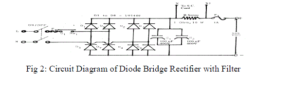
| A. Diode Bridge rectifier with filter |
| This circuit converts the available ac line voltage into required dc voltage for the next circuit. i.e. main power circuit. It uses four diode D1, D2, D3 and D4 in bridge configuration as shown in fig.2. Diode bridge converts ac to dc. This dc voltage is not pure dc voltage but contains ac ripples in it. So capacitor is connected across the output of the bridge rectifier which filters out ac contained in the dc and gives almost pure dc voltage. |
 |
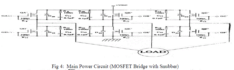
| The power circuit is a three phase bridge inverter using MOSFETs which converts dc power into ac power at desired output voltage and frequency. The center points of the transistor connection are used to take the output. Power MOSFET device permit the highest switching frequency although their power handling capability is limited. Their on state resistance increases approximately with the power of 2.6 as the blocking voltage increases, rendering the efficiency of high voltage MOSFET device low. Their typical ratings are about 50 A, 500V and 20KHz. |
| A basic three phase inverter is a six step bridge inverter with six semiconductor switching device. In inverter terminology, a step is defined as a change in the firing from one switch to other in proper sequence. For one cycle of 3600, each step would be of 600 interval for a six step inverter. |
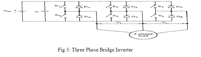 |
| Fig.3 shows the inverter with six semiconductor switched and the diodes. For simplicity the gating circuit are omitted. Let the three phase load be connected in star. These are two possible patterns of providing pulses to these switches. In one pattern, each switch conducts for 1800 and in the other each switch conducts for 1200. But in both these patterns gating signals are applied and removed at 600 intervals of the output voltage waveform. Therefore both these modes require a six step bridge inverter. |
| In this drive 1200 mode is used. The voltage waveforms and the firing sequence is shown in the fig. 3.4 (please refer fig. 3.4 on net page). It can be seen from the first row of the table that S1 conducts for 1200 and for the next 600, neither S1 nor S4 conducts. Now S4 is on at 1800 and it further conducts for 1200 i.e. unto 3000. This means that for 600 interval series connected switches do not conduct. At 3000 S4 is turned off, then 600 interval elapses before S1 is turned on again at 3600. |
 |
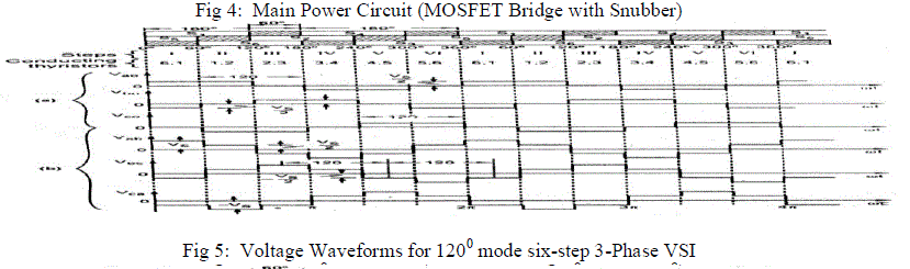 |
| In the second row, S2 is turned on at 1200 which conducts for 1200, then 600 interval elapses during which neither S2 and S5 conducts. At 3000, S5 is turned on and it conducts for 1200 after which S2 is turned on again with time interval of 600, in between. The third row is also completed similarly. The sequence in which the switches are fired is 1-6-2-4-3-5 and generate two step or quasi square wave format. During each step, only two switches conduct for this inverter-one from the upper group and one from the lower group. Any one of the load terminals always remains open in this case. in first step, the line to neutral voltages are given below. |
| Va0 = Vs / 2, V0b = Vs / 2 |
| Vb0 = Vs / 2 and Vc0 = 0 |
| The line voltage are given by |
| Vab = Va0 - Vc0 |
| Vbc = Vb0 - Vc0 |
| Vca = Vc0 - Va0 |
| It can be seen from the waveform that phase voltage have one positive pulse and one negative pulse (each of 1200 duration) for one cycle of output alternating voltage. The line voltage however, have six steps per cycle of output alternating voltage. The merits and demerits of 120-degree mode inverter over 180-degree mode inverter are as follows |
| i) In the 1800 mode inverter, when gate signal is cut off to turn off S1 at ïÃÂ÷t = 1800, gating signal for switch S4 is simultaneously applied to turn on S4 in the same leg. In practice a commutation interval must exist between the removal of first gating pulse and applications of the other pulse. Otherwise dc source would experience a direct short circuit through S1 and S4 in the same leg. |
| This difficulty is overcome considerably in 120-degree mode inverter. In this inverter, there is a 600 interval between the turning off of S1 and turning on of S4. The interval of 600 in between is sufficient for the commutation. In general, this angular interval of 600 exists between the turning off of one device and turning on of the complementary device in the same leg. |
| ii) In this mode of inverter, the potentials of only two output terminals connected to the dc source are defined at any time of the cycle. The potential of the third terminal, pertaining to the particular leg in which neither device is conducted is not well defined its potential therefore depends on nature of load circuit. Thus analysis of this type inverter circuit is complicated for a general load circuit. |
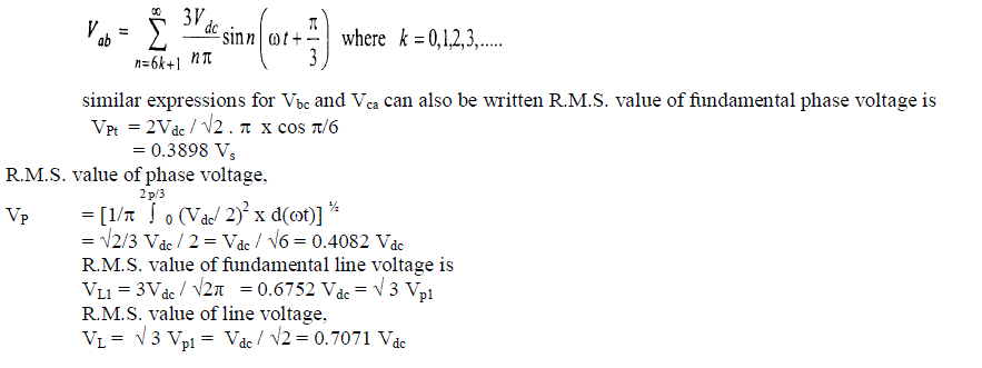
| The Fourier Analysis of line voltage waveform Vab shown in fig. |
 |
| C. Control Circuit |
| The control circuit consists of the clock signal generator, address generator for EPROM, data base stored in EPROM, logic circuits and optical solators. |
| Clock signal generator |
| It consists of timer 555 operated in as table mode. The clock generator runs at a very high frequency (256 times that of the output frequency). An astable multivibrator is a rectangular wave generating circuit is also called free running multivibrator as it dose not require external trigger to change the state of the output. Fig.3.6 shows the 555 timer connected in astable mode. |
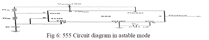 |
| The output of 555 is given as clock signal to the counter IC 7493 which generates the address lines for the EPROM. |
| i. Address Generator It consists of IC 7493 which is used for generating the address for the EPROM. This IC has four J-K flip flops with outputs Q0, Q1, Q2 and Q3. Q0 is the LSB and Q3 is the MSB. The flip-flops are shown arranged with LSB on the left. |
| Each flip-flop has a CP (clock pulse) input, which is just another name for the CLK input. The clock inputs to Q0 and Q1labeled CP0 and CP1 respectively, are externally accessible. The inversion bars over these inputs indicate that they are activated by a NGT. |
| Each flip-flop has an asynchronous CLEAR input, CD. These are connected together to the output of a two input NAND gate with input MR1 and MR2 where MR stands for Master Reset. Both MR inputs must be HIGH to clear the counter to 0000. |
| The logic diagram and symbol for 7493 is shown in fig (a) and (b). |
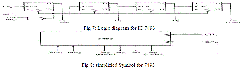 |
| Flip-flops Q1, Q2, and Q3 are already connected as a 3 bit ripple counter. Flip flop is not connected to anything internally. This allows the used the option of either connecting Q0 to Q1 to form a 4 bit counter or using Q0 separately if desired. |
| In the controller here, 2 such IC’s are used to generate 256 address lines as the data is stored in these locations. The output of these counter are respectively the address lines for the EPROM 2764. |
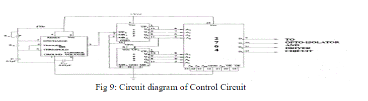 |
| ii. EPROM |
| The output generated by IC 7493 act as address lines for the EPROM wherein data base for the 1200 mode of conduction for the inverter is stored. An EPROM can be programmed by the user and it can also be erased and reprogrammed as often as desired. Once programmed, the EPROM is a non-volatile memory that will hold its stored data indefinitely. |
| The process of programming an EPROM involves the application of special voltage levels (typically in the 10-25 V) to the appropriate chip inputs for a specified amount of time range (typically 50 ms per address location). The programming process is usually performed by a special programming circuit that is separate from the circuit in which the EPROM will eventually be working. The complete programming process can take upto several minutes for one EPROM chip. |
| The data stored in EPROM is square pulse signal for 1200 mode. It is taken out by data line D0 to D5 . There are 13 address line, out of that only 8 (A0 to A7) address lines are used. |
| D. Isolator and driver circuit |
| Fig. shows isolator and driver circuit. Square wave pulses are available at the output of the control circuit. Which have phase relations as per the requirement. The power circuit is operating at very high voltage while control circuit is operating at very less voltage as compared to power circuit. So the control circuit ground and power circuit ground must be isolated from each other to protect control circuit from any damage due to malfunctioning in power circuit. It isolation is not used then it may be dangerous to operator. Also without isolation when gate pulses are applied the device become on and live terminal of supply is connected to ground of control circuit and power circuit. Any operation trying to control the circuit is likely to touch control ground (which is usually supposed to be the safest potential) and in fact is directly in contact with the live terminal of supply. Thus it is dangerous for the operation. This isolation is very much essential. |
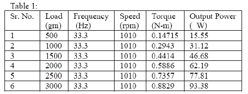
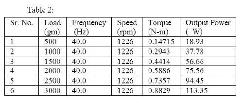
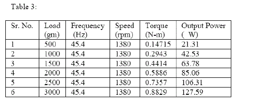
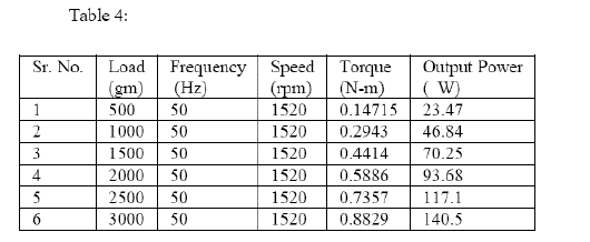
III.RESULTS ANALYSIS |
 |
 |
 |
 |
 |
 |
 |
| RESULT TABLE:- |
 |
 |
 |
 |
 |
 |
 |
IV. CONCLUSION |
| The Experiment results show that by varying the inverter frequency the speed of the motor also gets varied. If the frequency increases the speed of the motor also increases and if the frequency decreases the speed of the motor also decreases. If the frequency is kept constant at particular value, the speed of the motor also remains constant, irrespective of the load. Hence PMSM drive is suitable for Automotive Industry. |
References |
|