International Journal of Advanced Research in Electrical, Electronics and Instrumentation Engineering
ISSN ONLINE(2278-8875) PRINT (2320-3765)
ISSN ONLINE(2278-8875) PRINT (2320-3765)
Sunil Jadav, Munish Vashistaha,
|
| Related article at Pubmed, Scholar Google |
Visit for more related articles at International Journal of Advanced Research in Electrical, Electronics and Instrumentation Engineering
This paper presents a BSIM3v3.2.2 threshold model validation using SPICE simulations and mathematical models of BSIM are computed using MATLAB simulation and comparison between the mathematical and simulation model is presented. Further the short channel and narrow channel effects are analyzed and effect on threshold voltage is investigated.
Keywords |
| Threshold, Narrow channel, short channel, Threshold |
I. INTRODUCTION |
| The threshold voltage, commonly abbreviated as Vth, of a MOSFET is usually defined as the gate voltage where an inversion layer forms at the interface between the insulating layer (oxide) and the substrate (body) of the transistor. An accurate modelling of the threshold voltage is one of the most important requirements for precise description of device electrical characteristics. It also serves as a useful reference point for the evaluation of device operation regimes. By using threshold voltage, the whole device operation regime can be divided into three operational regions. Reverse short-channel effect (RSCE) is a result of non-uniform channel doping (halo doping ) in modern processes[1]. And helps in controlling the threshold voltage. First, if the gate voltage is greater than the threshold voltage, the inversion charge density is larger than the substrate doping concentration and MOSFET is operating in the strong inversion region and drift current is dominant. |
| Second, if the gate voltage is smaller than , the inversion charge density is smaller than the substrate doping concentration. The transistor is considered to be operating in the weak inversion (or sub threshold) region where diffusion current is now dominant [2 -7]. Lastly, if the gate voltage is very close to , the inversion charge density is close to the doping concentration and the MOSFET is operating in the transition region. As the channel length of MOSFETs is scaled down to deep-sub micrometer or sub-180 nm regime, short-channel effects, such as, steep threshold voltage roll-off, increased off-state leakage current and bulk punch through have been observed [2]. |
| In this work threshold voltage dependence investigated over Doping concentration (uniform & Non uniform), Short Channel effect and Narrow Channel effect [8] and detailed analysis of device is targeted with number of device parameters. |
| The paper is organized as section II presents previous model used by BSIM v.3.3 and in section III results are formulated and finally conclusion. |
II. BSIM THRESHOLD MODEL |
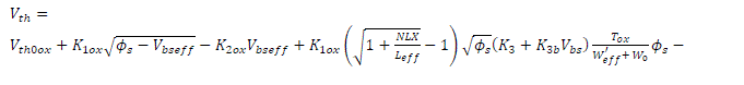
| For MOSFET’s with long channel length/width and uniform substrate doping concentration is given by [8]: |
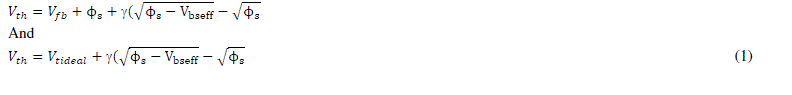 |
| Where is the flat band voltage and is the threshold voltage of the long channel device at zero substrate bias and γ is the body bias coefficient and is given by: |
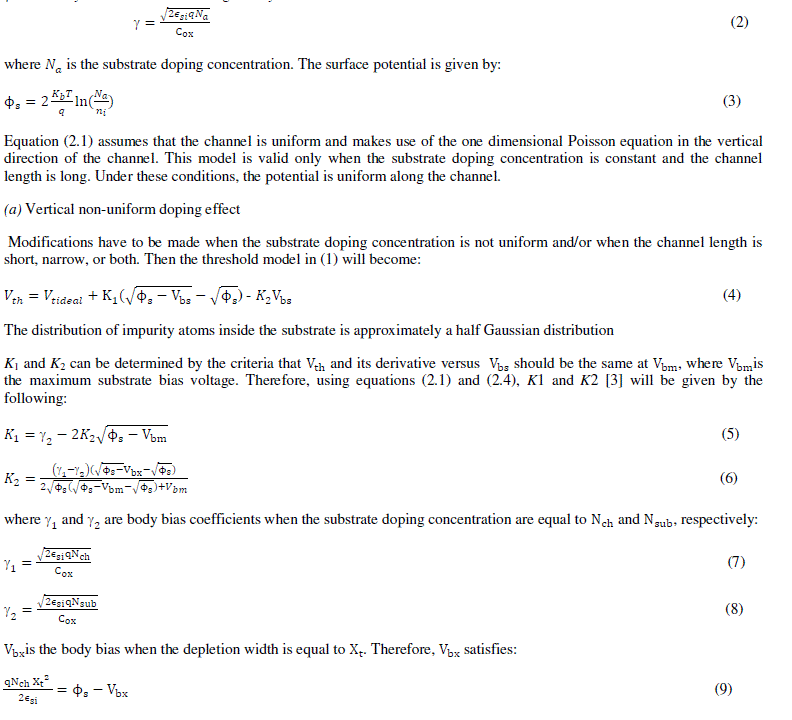 |
| (b) Lateral non-uniform doping effect |
| For some technologies, the doping concentration near the source/drain is higher than that in the middle of the channel. This is referred to as lateral non-uniform doping. As the channel length becomes shorter, lateral non-uniform doping will cause Vth to increase in magnitude because the average doping concentration in the channel is larger. The average channel doping concentration can be calculated as |
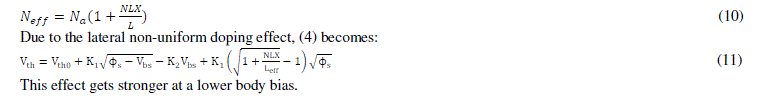 |
| This effect gets stronger at a lower body bias. |
| (c) Short Channel Effect |
| A MOS transistor is called a short-channel device if its channel length is on the same order of magnitude as the depletion region thicknesses of the source and drain junctions. Alternatively, a MOSFET can be defined as a short-channel device if the effective channel length is approximately equal to the source and drain junction depth . The short-channel effects that arise in this case are attributed to two physical phenomena: |
| (i) The limitations imposed on electron drift characteristics in the channel, |
| (ii) The modification of the threshold voltage due to the shortening channel length. |
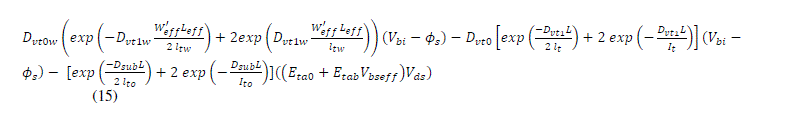
| The threshold voltage of a long channel device is independent of the channel length and the drain voltage. Its dependence on the body bias is given by (4). However, as the channel length becomes shorter, the threshold voltage shows a greater dependence on the channel length and the drain voltage. The dependence of the threshold voltage on the body bias becomes weaker as channel length becomes shorter, because the body bias has less control of the depletion region. The short-channel effect is included in the model as |
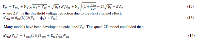 |
| (d) Narrow Channel Effect |
| Earlier, we have analysis the effect of Length that’s get short is referred to as short channel effect and now after the short channel the narrow channel effect is considered that is the width of the devices are getting narrow. Considering the NMOS device the actual depletion region in the channel is always larger than what is usually assumed under the one-dimensional analysis due to the existence of fringing fields [2]. This effect becomes very substantial as the channel width decreases and the depletion region underneath the fringing field becomes comparable to the "classical" depletion layer formed from the vertical field. The net result is an increase in |
 |
 |
III. RESULT & DISCUSSION |
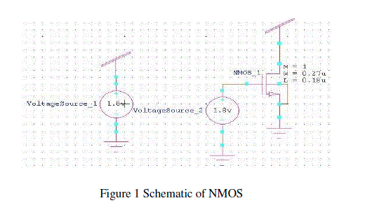
| The above approximated model is validated by using 180nm CMOS process parameters. Length and width of the device is taken as 180 nm and 270 nm and the temperature on which the device simulation is done i.e. 300 K. The supply voltage VDD is 1.8v and the gate to source input voltage maximum limit is set to 1.8v. And the DC analysis of the NMOS device is performed on the SPICE EDA tool. Figure 1 shows the schematic of NMOS used for simulation. |
 |
 |
 |
 |
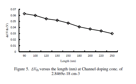 |
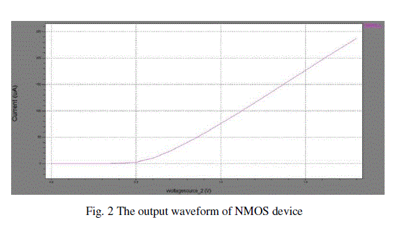
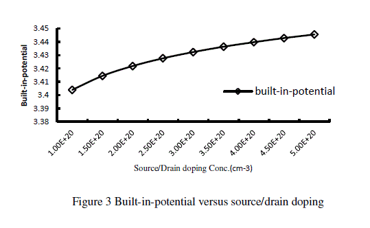
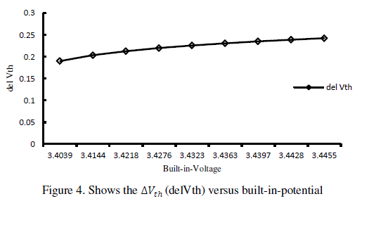
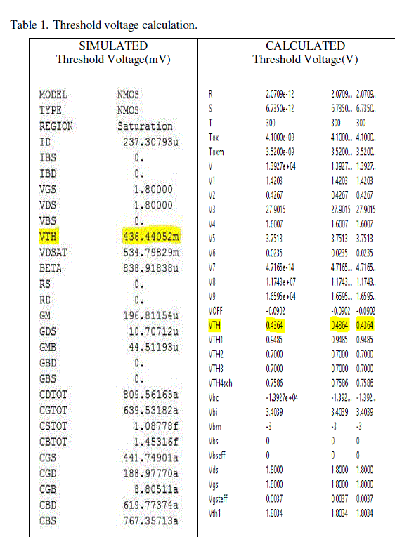
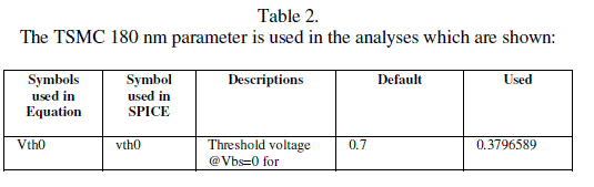
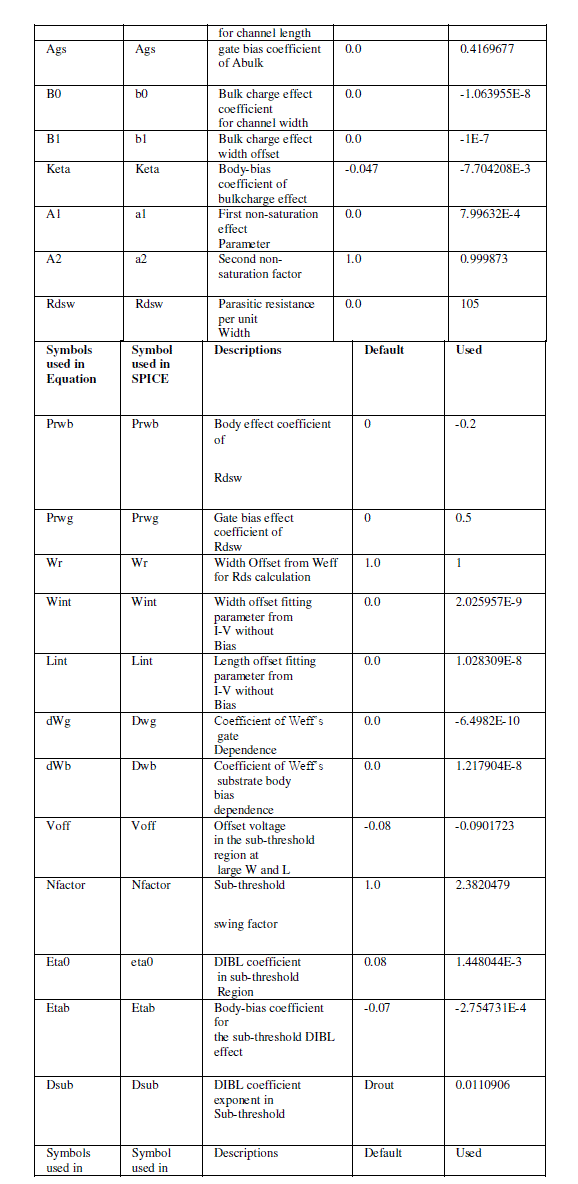
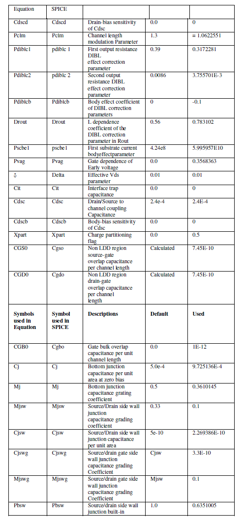
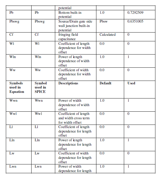
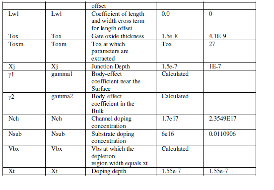
| The threshold voltage which is calculated by the SPICE and MATLAB simulator is shown in table 1. And is highlighted by yellow mark. And no of parameters used by MATLAB simulator is detailed in table 2. (with the default values of BSIM and used in this work). Figure 2 shows the threshold voltage at which NMOS device is ON. The above figure 3 reflects the effect on the built-in-potential ( ) versus source/drain doping concentration ( [8]. And is the threshold voltage reduction due to the short channel of the device. Now considering the variation in with respect to the built-in-Voltage. The relation between the and the built-in-Voltage is given by the (13) and relation between Vbi and is validated as shown in figure 4. If the parameter in the equation (13) are remain constant and the built-in-Voltage vary according to the formulation they are directly related to each other as built-in-Voltage increases the increases and similarly if the built-in-Voltage decrease the will decrease. Further w.r.t. to length of device the BSIM model is validated.The parameter Length is the major parameter in the sub-micron technology as the technology moving toward the sub-micron the Length of the device getting shorter so the impact of the length on the is expressed graphically in figure 5. The is the function of length according to the equation (13) that means the depend upon the length as the length of the device is increases the will decrease. One major consideration is that the channel doping concentration is 2.8469e-18cm-3. |
IV.CONCLUSION |
| Based on device parameters approximation the mathematical models of BSIM3v3.2.2 threshold model is validated with the SPICE simulations. The threshold voltage calculated is 0.436V and it is 98% close to the simulated model. Scaling effect is also investigated in terms of short Channel Effect. And the increase in the length the is increased and resulted threshold voltage is decreased. |
| Further it is also concluded that the first order coefficient of the Narrow channel shows the decrease in the threshold voltage but the second coefficient and has a negligible effect on the threshold voltage. This work will help to the users of VLSI modelling i.e how to work with 49 and 57 Level MOS parameters. |
References |
|
 |
 |
 |
 |
 |
 |
 |