International Journal of Advanced Research in Electrical, Electronics and Instrumentation Engineering
ISSN ONLINE(2278-8875) PRINT (2320-3765)
ISSN ONLINE(2278-8875) PRINT (2320-3765)
| Mukesh Gupta1, Sachin Kumar2, Vagicharla Karthik2 |
| Related article at Pubmed, Scholar Google |
Visit for more related articles at International Journal of Advanced Research in Electrical, Electronics and Instrumentation Engineering
In this paper a method of generating regulated dc voltage with linear transfer characteristics is suggested. The dc output voltage which is proportional to control voltage can be obtained using Cosine Control firing scheme. Present paper deals with design, fabrication and testing of cosine control firing scheme for single phase half controlled rectifier with desired results simulated in MATLAB/Simulink and simulation results are verified experimentally for different types of loads..
Keywords |
| Cosine control scheme, half controlled bridge rectifier, control voltage, MATLAB, isolation circuit, monostable. |
INTRODUCTION |
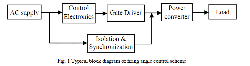
| Single phase bridge rectifiers utilize thyristor or silicon controlled rectifier (S.C.R.) as switching devices which is explained in [1]-[4]. To turn on a thyristor, various control schemes are used to generate gate pulses or firing pulses which are supplied between gate and cathode of the thyristor [2]. The number of degrees from the beginning of the cycle when the thyristor is gated or switched on is referred to as the firing angle, α and when the thyristor is turned off is known as extinction angle, ïÃÂâ as discussed in [5], [6]. The thyristors of bridge rectifier are switched on and off in proper sequence by using control electronics and gate driver circuits to get a controlled dc output voltage. For this a sinusoidal ac voltage is supplied to control circuit and the same supply is given to bridge rectifier circuit through isolation and synchronization block as shown in Fig. 1. This paper implements control electronics circuit by using the cosine control firing scheme and the controlled dc output voltage thus obtained from the bridge rectifier is effectively utilized for resistive and motor loads. |
 |
II. COSINE CONTROL SCHEME |
| Conventionally, ramp and cosine firing schemes are used for generating the gate pulses [5], [7]. The cosine control firing scheme has an advantage that it linearizes the transfer characteristic of bridge rectifier by using an indirect control variable as a substitute for firing angle, α as given in (1) and (2) [8]. This scheme also provides automatic negative feedback to the change in input ac supply. The input ac voltage of peak value, Vm is transformed to a low level ac voltage, Vao of 9 V is obtained by using a 230/9 V, 50 Hz step down transformer. The cosine wave generator integrates Vao to obtain a cosine wave of peak value, Em which is compared with a variable dc control voltage, EC by using a comparator. The comparator output is fed to monostable block. The monostable output is modulated at high frequency to obtain the firing pulses. After proper amplification and isolation, these firing pulses are supplied to the thyristors of the bridge rectifier circuit. |
| The firing angle, α is given by - |
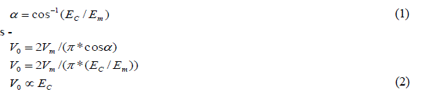 |
| The block diagram of implemented cosine control firing scheme is shown in Fig. 2 and the utility of each module is explained below [8], [9]. |
 |
| A. Cosine Wave Generator |
| Cosine wave generator uses an op-amp along with resistors and capacitors to realize the integrator function. It provides a phase shift of 900 to the input voltage Va0 and thus a cosine wave is obtained |
| B. DC Control Voltage |
| The dc control voltage, EC that can be varied between ± 12 V is used to vary the firing angle, α ranging from 0 0 to 1800. The ground point of the dc supply is connected to the common ground point zero of the transformer |
| C. Comparator |
| An op-amp is used as comparator. The variable dc voltage is applied to the non-inverting terminal and the cosine wave is applied to the inverting terminal of the comparator. |
| D. Monostable |
| The square wave output of the comparator is fed as input to the monostable multivibrator which gives two complementary outputs, Q and QâÃâ¬ÃŸ each of 10 ms duration. These complementary outputs are primary firing pulses which are modulated to trigger the thyristors. The time period, T of monostable multivibrator is given in (3). |
| where R and C are the resistance and capacitance used. |
| E. Carrier Wave |
| Pulse gating of thyristor is not suitable for RL loads, this difficulty can be overcome by using continuous gating. However, continuous gating may lead to increased thyristor losses and distortion of output pulse. So, a pulse train generated by modulating the pulse gate at high frequency is used to trigger the thyristor. This high frequency wave is known as carrier wave and is generated by using astable multivibrator. |
| F. AND |
| AND operation is performed between monostable outputs and carrier wave thus pulses required for triggering the thyristors called firing pulses or gate pulses are obtained. |
| G. Pulse Amplification and Isolation Circuitry |
| The gate pulses obtained from AND operation may not be able to turn on the thyristor [10]. It is therefore common to feed these gate pulses to a pulse amplification and isolation circuitry to meet the two objectives of strengthening these pulses and providing proper isolation. |
III. BRIDGE RECTIFIER |
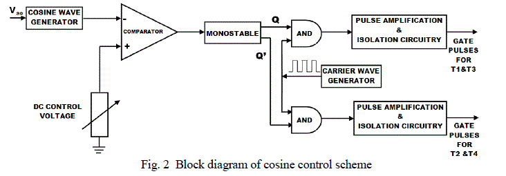
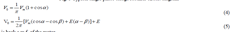
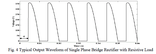
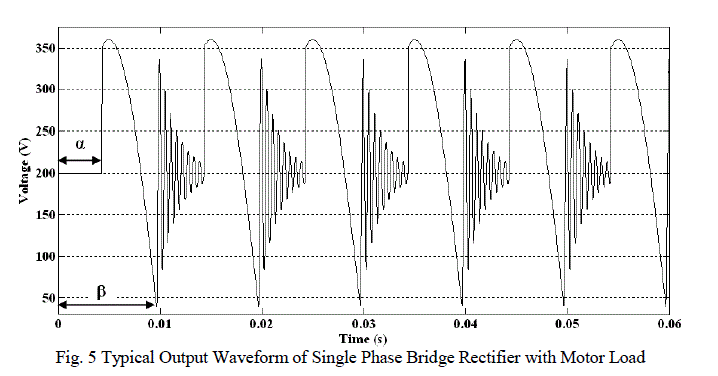
| The typical single phase half controlled bridge rectifier circuit consists of two thyristors and two diodes T1, T2, and D1 and D2 as shown in Fig. 3. The generated gate pulses are supplied between gate, G and cathode, K to trigger T1 during positive half cycle and T2 during negative half cycle of ac supply voltage [4]. The typical controlled dc output voltage waveforms for resistive and motor loads are shown in Fig. 4 and Fig. 5. The expression of average output voltage, V0 as a function of firing angle, ïÃÂá and extinction angle, ïÃÂâ with resistive load and motor load are given in (4) and (5) respectively. |
 |
 |
| 'E' is back e.m.f. of the motor. |
 |
 |
IV. RESULTS |
| The cosine control firing pulses are supplied to single phase bridge rectifier circuit and the controlled dc output voltage is used to drive the resistive and motor loads. The voltage waveforms at different stages of control circuit and output of the bridge rectifier circuit as simulated in matlab/simulink are discussed. Afterwards the experimental results are also compared with simulation results |
| A. Cosine Control Scheme |
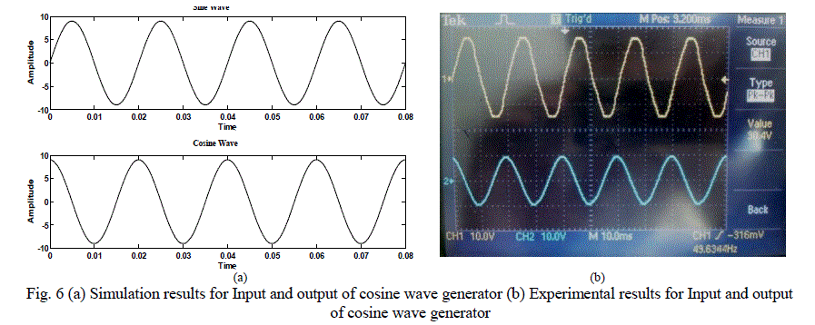
| 1) Cosine Wave Generator: The simulation results and experimental outputs of the cosine wave generator are shown in Fig. 6 (a) and Fig. 6(b) respectively. The upper half shows an input sine wave and lower half indicates the cosine wave. |
 |
| 2) Comparator: The simulation results and experimental outputs of the comparator are shown in Fig. 7 (a) and Fig. 7 (b) respectively. The lower half shows the square output voltage which is obtained by comparing cosine wave and DC control voltage. |
| 3) Monostable: The square wave output of the comparator is fed to the monostable multivibrator. The simulation results and experimental outputs of the monostable multivibrator are shown in Fig. 8 (a) and Fig. 8 (b) respectively. The lower and upper halves indicate two output waves each of 10 ms duration and are complement to each other |
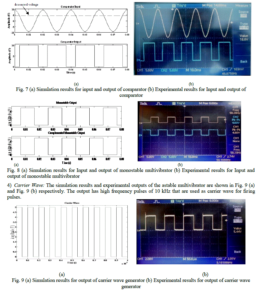 |
| 5) AND Operation: The outputs of the monostable multivibrator are superimposed on the carrier wave using AND operation. The corresponding simulation and experimental results are shown in Fig. 10 (a) and Fig 10 (b) respectively. The lower and upper halves indicate two outputs each of 10 kHz frequency and 10 ms duration and are complement to each other. |
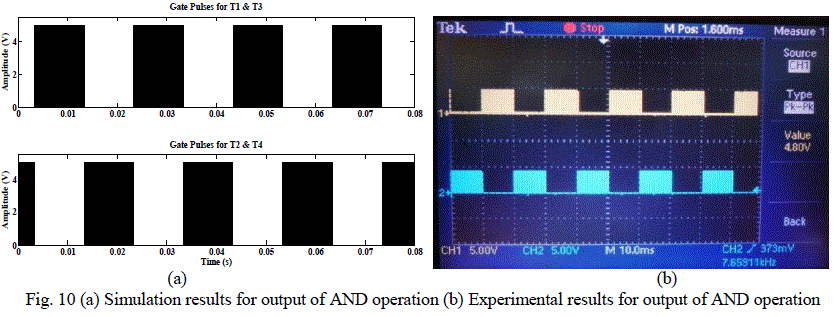 |
| 6) Pulse Amplification and Isolation Circuitry: The firing pulses obtained previously are amplified and isolated and experimental results are shown in Fig. 11. |
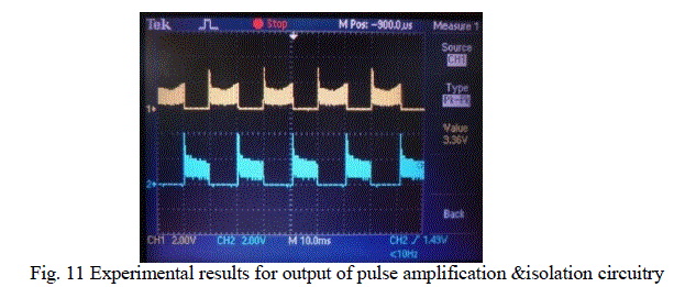 |
| B. Bridge Rectifier Output for Resistive Load |
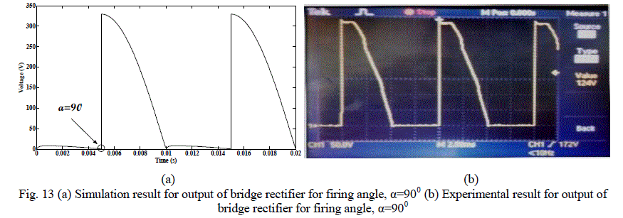
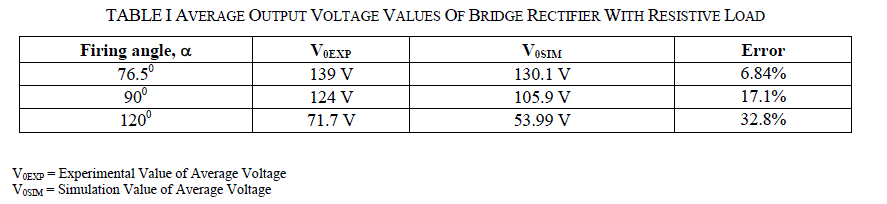
| 1) for firing angle, α = 76.50 The simulation results and experimental outputs of the bridge rectifier with resistive load are shown in Fig. 12 (a) and Fig 12 (b) respectively. The value of average output voltage for simulation as well as for experimental results is given in Table I. |
 |
| 2) for firing angle, α = 900 |
| The simulation results and experimental outputs of the bridge rectifier with resistive load are shown in Fig. 1 (i) and Fig 1(ii) respectively. The value of average output voltage for simulation as well as for experimental results is given in Table I. |
 |
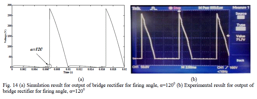
| 3) for firing angle, α = 1200 |
| The simulation results and experimental outputs of the bridge rectifier with resistive load are shown in Fig. 14 (a) and Fig. 14 (b) respectively. The value of average output voltage for simulation as well as for experimental results is given in Table I. |
| It is seen from the above discussion that the theoretical value is slightly less than the practical value which is due to the internal inductance of practical circuit. |
 |
 |
| C. Bridge Rectifier Output for Motor Load |
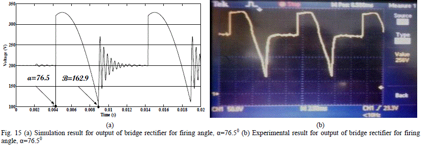
| 1) for firing angle, α = 76.50 |
| The simulation results and experimental outputs of the bridge rectifier with motor load are shown in Fig. 15 (a) and Fig. 15 (b) respectively. The value of average output voltage for simulation as well as for experimental results is given in Table II |
 |
| 2) for firing angle, α = 900 |
| The simulation results and experimental outputs of the bridge rectifier with motor load are shown in Fig. 16 (a) and Fig. 16 (b) respectively. The value of average output voltage for simulation as well as for experimental results is given in Table II |
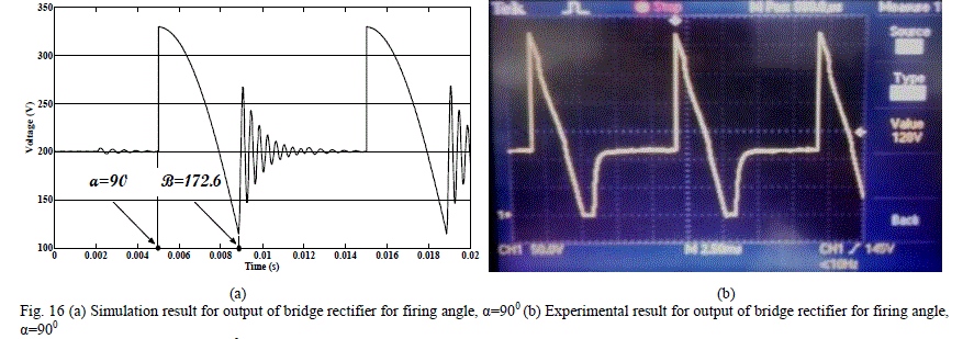 |
| Fig. 16 (a) Simulation result for output of bridge rectifier for firing angle, α=900 (b) Experimental result for output of bridge rectifier for firing angle, α=900 |
| 3) for firing angle, α = 1200 |
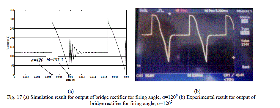
| The simulation results and experimental outputs of the bridge rectifier with motor load are shown in Fig. 17 (a) and Fig. 17 (b) respectively. The value of average output voltage for simulation as well as for experimental results is given in Table II. |
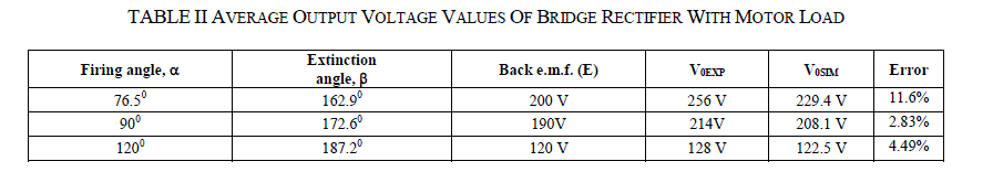 |
| V0EXP = Experimental Value of Average Voltage V0SIM = Simulation Value of Average Voltage |
 |
V. CONCLUSION |
| Gate pulses obtained by cosine control scheme have been effectively utilized to control the dc output single phase half controlled bridge rectifier on both resistive load and motor load. The present control scheme provides linear control transfer characteristics between input and output i.e., firing angle is directly proportional to the dc control voltage. The experimental results are in coordination with the simulation results. Thus, presented control scheme can be successfully utilized to get the controlled dc voltage for industrial applications. |
| In order to produce steady and smooth DC, a filter may be introduced at the output [7]. Pulse amplification and isolation circuitry may be replaced by driver ICs. |
| Monostable are may be replaced by zero-crossing detector and AND gates to avoid the false triggering due to output bouncings [11]. |
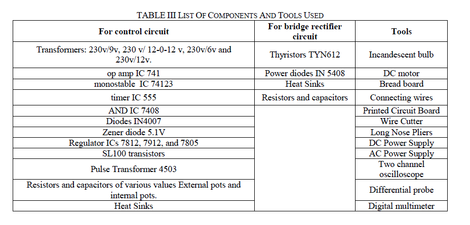
APPENDIX |
 |
 |
ACKNOWLEDGMENT |
| Authors whole heartedly thank to G.B. Pant Engineering College for providing an opportunity to compose an international journal paper on thyristor firing which is emerging trend in power electronics. Authors take this opportunity to express their gratitude towards Mr. V.M. Mishra (Head of Electrical Engineering Department, G.B.P.E.C. Pauri) for providing us the valuable facilities. Authors would like to thank all their colleagues for their support. Last but not least authors would like to thank all the departments of G.B.P.E.C. Pauri for their physical, emotional and intellectual support especially precious suggestions in need. |
References |
|