International Journal of Advanced Research in Electrical, Electronics and Instrumentation Engineering
ISSN ONLINE(2278-8875) PRINT (2320-3765)
ISSN ONLINE(2278-8875) PRINT (2320-3765)
V.Kamalakannan1, Shilpakala.V2, Ravi.H.N3
|
| Related article at Pubmed, Scholar Google |
Visit for more related articles at International Journal of Advanced Research in Electrical, Electronics and Instrumentation Engineering
Reversible logic has extensive applications in quantum computing, it is a unconventional form of computing where the computational process is reversible, i.e., time-invertible. The main motivation behind the study of this technology is aimed at implementing reversible computing where they offer what is predicted to be the only potential way to improve the energy efficiency of computers beyond von Neumann-Landauer limit. It is relatively new and emerging area in the field of computing that taught us to think physically about computation Quantum Computing will be a total change in how the computer will operate and function. The reversible arithmetic circuits are efficient in terms of number of reversible gates, garbage output and quantum cost. In this paper design Reversible Binary Adder- Subtractor- Mux, Adder-Subtractor- TR Gate., Adder-Subtractor- Hybrid are proposed. In all the three design approaches, the Adder and Subtractor are realized in a single unit as compared to only full adder/subtractor in the existing design. The performance analysis is verified using number reversible gates, Garbage input/outputs and Quantum Cost.The reversible 4-bit full adder/ subtractor design unit is compared with conventional ripple carry adder, carry look ahead adder, carry skip adder, Manchester carry adder based on their performance with respect to area, timing and power. Hence the proposed work is useful in low power applications where both adder and subtractor units are required
Keywords |
| Reversible gates, Fredkin gate, Feynman gate, Toffoli Gate, Peres gate. |
I.INTRODUCTION |
| Reversible logic has applications in Nanotechnology, quantum computing, Low power CMOS, Optical computing and DNA computing, etc., one of the important applications of the reversible logic is quantum computation. Reversible circuits are those circuits that do not lose information and reversible computation in a system can be performed only when system comprises of reversible gates. |
| Most of the gates used in digital design are not reversible for example the AND, OR and EXOR gates does not perform reversible operation. A reversible circuit/gate can generate unique output vector from each input vector, and vice versa, that is there is a one to one mapping between the input and output vectors. Therefore, of the commonly used gates only the NOT gate is reversible. |
| Energy loss is an important consideration in digital design. Part of the problem of energy dissipation is related to non ideality of switches and materials. A set of reversible gates are needed to design reversible circuit. Several such gates are proposed over the past decades. Reversible gates are the building blocks for reversible circuits, having the following characteristics. |
| A reversible gate has its input and output with a one to one correspondence. That is the inputs of a reversible gate can be uniquely determined from its outputs. |
| A reversible logic gate must have an equal number of inputs and outputs |
| The fan out of every signal including primary inputs in a reversible gate must be one. |
| Classical logic synthesis methods cannot be directly applied to design reversible logic circuit. |
| One of the most important features of a reversible gate is its garbage output. Every gate output that is not used as input to other gate or as a primary output is called garbage output. Simply to say an unutilized output from a gate is garbage. |
| Each reversible gate has a cost associated with it called quantum cost. The quantum cost of a reversible gate is the number of 2x2 reversible gates or quantum logic gates required in designing it. |
II. INTRODUCTION TO REVERSIBLE GATE |
| The simplest reversible gate is NOT gate and is a 1x1 gate. Controlled NOT (CNOT) gate is an example for a 2x2 gate. There are many 3x3 reversible gates such as Fredkin gate, Toffoli gate, Peres gate and TR gate. Each reversible gate has a cost associated with it called quantum cost. The quantum cost of 1x1 reversible gates is zero, and quantum cost of 2x2 reversible gates is one. Any reversible gate is realized by using 1x1 NOT gates and 2x2 reversible gates, such as V and V+ (V is square root of NOT gate and V+ is its hermitian) and Feynman gate which is also known as controlled NOT gate (CNOT). The V and V+ quantum gates have the following property: |
| V x V = NOT |
| V x V+ = V+ x V = I |
| V+ x V+ = NOT. |
| The quantum cost of a reversible gate can be calculated by counting the number V, V+ and CNOT gates used in implementing it except in few cases. |
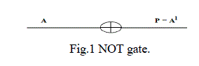
| 2.1 NOT Gate |
| This is the only reversible gate among the conventional logic gates. This is a 1x1 gate with quantum cost of zero. |
 |
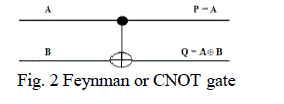
| 2.2 Feynman Gate (CNOT gate) |
| This is a 2x2 gate having mapping (A, B) to (P=A, Q=A B) where A, B are inputs and P, Q are outputs respectively. Since it is 2x2 gate it has a quantum cost of one. |
 |
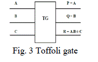
| 2.3 Toffoli Gate |
| This is a 3x3 reversible gate with two of its outputs are same as inputs with the mapping (A, B, C) to (P=A, Q=B, R= A.B C). Where A, B, C are inputs and P, Q, R outputs respectively. Toffoli gate is one of the most popular reversible gates and has quantum cost of 5. It requires 2V gates, 1 V+ gate and 2 CNOT gates. |
 |
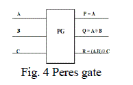
| 2.4 Peres Gate |
| Peres gate is a three input and three output (3x3) reversible gate having the mapping (A, B, C) to (P=A, Q= A B, R= (A.B) C), where A, B, C are the inputs and P, Q, R are the outputs, respectively. Peres gate has the quantum cost of 4, since it requires 2 V+ gate, 1 V gate and 1 CNOT gate. Among 3x3 reversible gates, this has the minimum quantum cost. |
 |
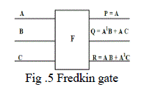
| 2.5 Fredkin Gate |
| Fredkin gate is a 3x3 conservative reversible gate. It maps (A, B, C) to (P=A, Q= A' B+AC, R=AB+ A'C), where A, B, C are the inputs and P, Q, R are the outputs, respectively. Fredkin gate can be implemented with a quantum cost of 5 and it requires 2 dotted rectangles, 1 V gate and 2 CNOT gates. |
 |
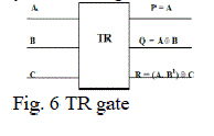
| 2.6 TR Gate |
| TR gate has 3 inputs and 3 outputs having inputs and outputs mapping as (P = A, Q=A B, R=(A . B') C), where A, B, C are the inputs and P, Q, R are the outputs, respectively. TR gate may also be realized in a different implementation with quantum cost of 6 or lesser than 6. Therefore it is considered that the quantum of TR gate as 6 for the calculation of parallel Subtractor implementing by reversible gate |
 |
III.INTRODUCTION TO REVERSIBLE GATE DESIGN |
| Reversible circuit/gate can generate unique output vector from each input vector, and vice versa, i.e., there is a one to one correspondence between the input and output vectors. Thus, the number of outputs in a reversible gate or circuit has the same as the number of inputs, and commonly used traditional NOT gate is the only reversible gate. Each Reversible gate has a cost associated with it called Quantum cost. The Quantum cost of a Reversible gate is the number of 2*2 Reversible gates or Quantum logic gates required in designing. One of the most important features of a Reversible gate is its garbage output i.e., every input of the gate, which is not used as input to other gate or as a primary output is called garbage output. |
| 3.1 Reversible Logic Gates |
| A reasonable computation is one that may be written in terms of some (possibly large) Boolean expression, and any Boolean expression may be constructed out of a fixed set of logic gates. Such a set (e.g., AND, OR and NOT) is called universal. In fact we can get by with only two gates, such as AND and NOT or OR and NOT. Alternatively, we may replace some of these primitive gates by others, such as the exclusive-OR (called XOR); then AND and XOR form a universal set. Any machine, which can build up arbitrary combinations of logic gates from a universal set is then a universal computer. Which of the above gates is reversible? Since AND, OR, and XOR are many-to-one operations, they are not logically reversible. Before we discuss how these logic gates |
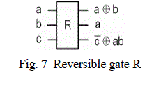
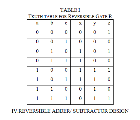
| Several reversible gates have been proposed over the years, e.g., the Toffoli gate, the Fredkin gate etc. A 3-input and 3-output reversible logic gate was proposed in. It has inputs a, b, c and outputs x, y and z as shown in Fig 7. The truth table of the gate is shown in the Table 1. It can be verified from the truth table that the input pattern corresponding to a particular output pattern can be uniquely determined. The gate can be used to invert a signal and also to duplicate a signal. The signal duplication function can be obtained by setting input b to 0. The EX-OR function is available at the output x of the gate. The AND function is obtained by connecting the input c to 0, the output is obtained at the terminal z. An OR gate is realized by connecting two new reversible gates. |
 |
 |
| 4.1 Adder circuits |
| Several types of adders are used in computing systems. A ripple carry adder has the simplest structure. In a ripple carry adder, full adders connected in series generate the sum and the carry outputs based on the addend bits and the carry input. The disadvantage of a ripple carry adder is that the carry has to propagate through all stages. |
| 4.2 Ripple carry adders |
| The basic building block of a ripple carry adder is a full adder block. A full adder computes the sum bit Si and the carry output c i+1 based on addend inputs a and b and carry input c. The output expressions for a ripple carry adder are |
| (1) Si = a xor b xor c; |
| (2) Ci+1 = ab + bc + ca; (i = 0,1,2,….) |
| A Reversible circuit/gate can generate unique output vector from each input vector, and vice versa, i.e., there is a one to one correspondence between the input and output vectors. Thus, the number of outputs in a reversible gate or circuit has the same as the number of inputs, and commonly used traditional NOT gate is the only reversible gate. Each Reversible gate has a cost associated with it called Quantum cost. The Quantum cost of a Reversible gate is the number of 2*2 Reversible gates or Quantum logic gates required in designing. One of the most important features of a Reversible gate is its garbage output i.e., every input of the gate which is not used as input to other gate or as a primary output is called garbage output. Minimization of the number of Reversible gates, Quantum cost and garbage inputs/outputs are the focus of research in Reversible logic. |
| 4.2 Proposed Reversible Adder / Subtractor unit |
| The design approach followed here mainly focuses on the reversible full adder and subtractor together in a single unit. Three types of full adder/subtractor implementations have discussed and the performance of each designs have been compared in terms of the number of reversible gates used, number of garbage inputs/outputs and the quantum cost. A four-bit parallel adder/subtractor is built using the full adder/subtractor and half adder/subtractor units. Four-bit parallel subtractor is designed using all the three types of adder/subtractor units. |
 |
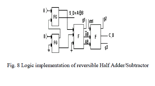
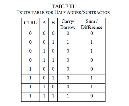
| 4.3 Half Adder – Subtractor |
| Reversible half adder/subtractor logic is implemented with the four reversible gates of which two are Fredkin and two are Feynman gates. The numbers of garbage outputs are three, garbage inputs are two and quantum cost is twelve. This implementation is as shown in figure15. This half adder/subtractor is used in implementing four-bit parallel reversible adder/subtractor unit. |
 |
 |
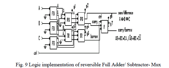
| 4.4 Full Adder-Subtractor-Mux |
| This design is based on the utilization of appropriate reversible gates for each function namely, Peres gate for adder function, TR gate for substractor function and Fredkin gate for multiplexing the Carry and Borrow line into single line output. 3 Feynman gates are used for creating the necessary signal multiplication (buffering) of each input signal. This design uses 8 reversible gates, 3 Feynman gates, 2 Peres gates, 2 TR gates and one Fredkin gate. As shown in the table 1 there are 7 garbage outputs5 garbage (constant) inputs and the total quantum cost is 28. This implementation is as shown in fig. 9. |
 |
| This logic is implemented using VHDL code and simulated using Modelsim simulator. The individual gates functionality is implemented using Behavioral style of modeling and the overall logic is implemented using structural style of modeling. |
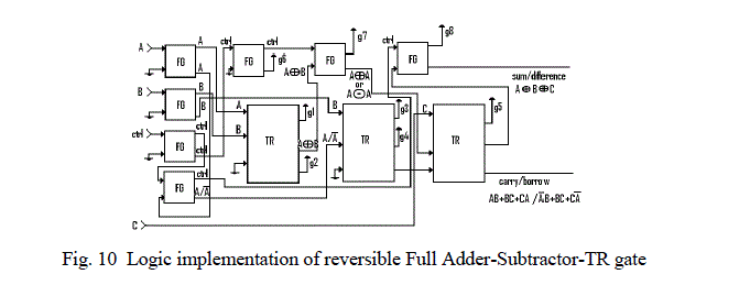
| 4.5 Full Adder-Subtractor-TR gate |
| In this design the main functionality of addition and substraction is realized by using only TR gates. Feynman gates are used for input signal buffering. The design utilizes 3 TR gates and 6 Feynman gates, in total 9 gates. The garbage output in this design is 7 and the garbage inputs are 5. The quantum cost for the design is 24. Even though one additional Feynman gate (C-NOT Gate) is used in this design, a quantum cost advantage of 4 is obtained when compared to the Adder-Substractor-Mux design. This quantum cost advantage is mainly due to the realization of arithmetic blocks of adder and substractor is realized with 3 TR gates as against the 5 numbers of 3x3 reversible gates for Adder-Sustractor-Mux design. (Two Pearson gates, two TR gates and one Fredkin gate). This implementation is as shown in fig.10. |
 |
| This logic is implemented using VHDL code and simulated using Modelsim simulator. The individual gates functionality is implemented using Behavioral style of modeling and the overall logic is implemented using structural style of modeling. |
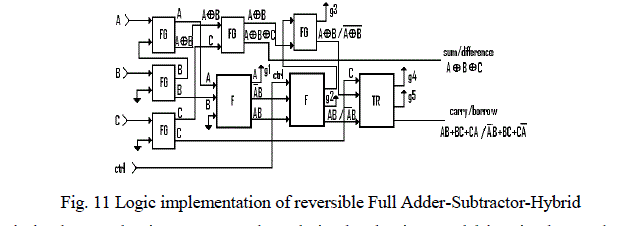
| 4.6 Full Adder-Subtractor- Hybrid |
| This is an optimized implementation of adder-substractor function. The sum/difference output is realized in this case with two Feynman gates. To realize the carry borrow line we utilized two Fredkin gates and a TR gate. This design, in total utilizes 8 gates including the C-NOT gates for input signal multiplication. The garbage output is 5 and garbage input in this design is 3. The quantum cost is 21. The optimization in terms of the garbage input, garbage output and quantum cost in this case is obtained due to optimal utilization of gates. The sum/difference function in this case is realized with just two CNOT gates. Therefore it is essential to have a design approach where, the required functionality may be realized with simplest gates as much as possible. We could not realize the carry/borrow function with simple 2x2 gates effectively. So, we utilized 3x3 gates for the realization. Many algorithms are available in literature. To synthesize the reversible logics, one of the basic goals of these algorithms is to realize the required function with simplest possible gates. This implementation is as shown in fig. 11. |
 |
| This logic is implemented using VHDL code and simulated using Modelsim simulator. The individual gates functionality is implemented using Behavioral style of modeling and the overall logic is implemented using structural style of modeling. |
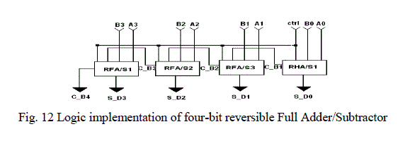
| 4.7 Four-Bit reversible Parallel Adder/Subtractor unit |
| A four-bit reversible parallel adder/subtractor is built using the full adder/subtractor and half adder/subtractor units. Four-bit parallel adder/subtractor is designed using all the three types of adder/subtractor units. This implementation requires three full adder/subtractor blocks and one half adder/subtractor blocks. These implementation is been done using VHDL code and verified for its functionality. |
 |
| V. RESULT AND DISCUSSION |
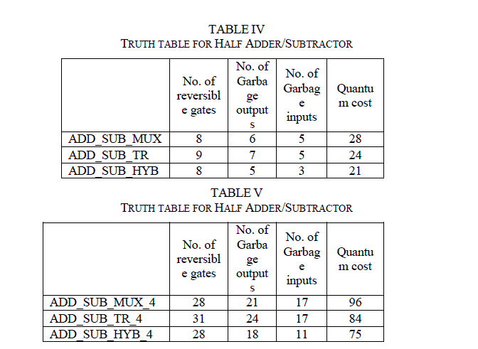
| Implementations of three types of reversible full adder/subtractor are coded in VHDL and simulated using ModelSim simulator. The functionality is verified. A comparison of the implementations based on the number of gates used, number of garbage inputs/outputs and quantum cost of the logics is as shown in the Table IV. |
| Reversible four-bit parallel adder/subtractor implementations in all the three types are verified. A structural model coding is used to build four-bit parallel adder/subtractor with three full adder/subtractor and one half adder/subtractor blocks. The functionality is verified. A comparison of the implementations based on the number of gates used, number of garbage inputs/outputs and quantum cost of the logics is as shown in the table V |
 |
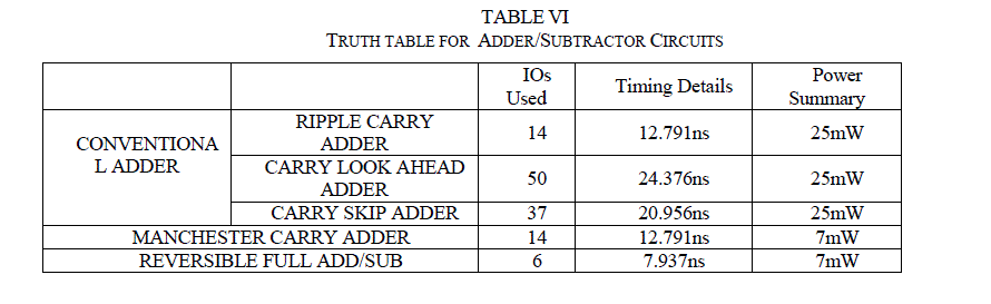
| Comparison of Optimization Results of reversible Full Adder/Subtractor design with Conventional Ripple carry adder, carry look ahead adder, carry skip adder manchhester carry adder with respect to area, timing and power is shown in Table VI. |
 |
VI.CONCLUSION |
| Successfully designed three types of reversible full adder/subtractor unit and compared their performance in terms of number of gates used, garbage inputs/outputs and quantum cost. Many algorithms are available in literature to realize the reversible logic; one of the basic goals of these algorithms is to realize the required function with the simplest possible reversible gates. Out my three designs full adder-subtractor-hybrid implementation is optimized as it utilizes appropriate gates to realize the required functions of the unit. Also four-bit reversible parallel adder/subtractor is implemented and performance in terms of number of gates used, garbage inputs/outputs and quantum cost are compared |
References |
|