International Journal of Advanced Research in Electrical, Electronics and Instrumentation Engineering
ISSN ONLINE(2278-8875) PRINT (2320-3765)
ISSN ONLINE(2278-8875) PRINT (2320-3765)
Hazli Rafis1, Hamidon A.H2, M.Y. Azdiana1, A.Jaafar3, A.A. Latiff4, H.H.M. Yusof1, W.H.M. Saad5
|
| Related article at Pubmed, Scholar Google |
Visit for more related articles at International Journal of Advanced Research in Electrical, Electronics and Instrumentation Engineering
Design of DC-DC Boost Converter for boosting voltage from Thermoelectric Cooler (TEC) with high temperature is demonstrated. Since TEC generates very small voltages from 0.2 V to 0.8V, the use of passive components is not reasonable. In this design, an integrated circuit (IC) MAX 757 is introduced as DC-DC boost converter. The MAX757 can boost input voltage down to 0.7 V and generates a higher adjustable output voltage in the range from 2.7 V to 5.5 V. The ability of the designed circuit was verified at various temperatures and the output voltages were analyzed. Simple in design and low in cost, the circuit can boost small voltages from TEC in a convenient way. Thus, this designed circuit will be very promising in powering up small electronic applications such as sensor circuits in monitoring systems.
Keywords |
| Thermoelectric cooler (TEC), DC-DC boost converter and temperature |
I.INTRODUCTION |
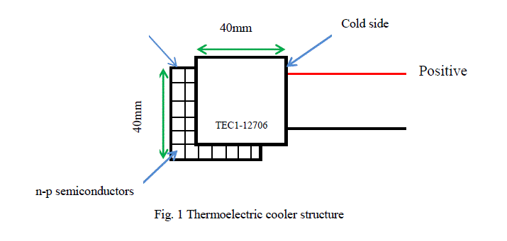
| Currently, the use of energy harvesting technique has a vast potential in energy market. This is due to its advantages in term of green technology. TEC is a device that converts thermal energy directly into electrical based on thermalelectric conversion called Seebeck Effect [1]. TEC may offer many advantages such high reliability, small size, long life, having no moving parts and being environmentally friendly compared to conventional electrical power generators. Fig. 1 shows the structure of the TEC (TEC1-12706) used in this design as a power source generator. The TEC structure consists of thermoelectric materials which are sandwiched by two heat exchanger plates at its two ends respectively. One of the two exchangers has high temperature, and hence, it is called hot side of TEC. The other has low temperature and is called cold side of TEC. The different in temperature between two exchangers causes a continuous current flow in the conductor. |
| Basically, DC-DC boost converter involves the storage of electrical energy into components, such as capacitors and inductors, and the release of energy to loads. By controlling the time for energy storage and release, the average voltage level appear in the converter load can be controlled. The average load voltage level can thus be either higher or lower than the voltage level of the power source. The rotation of energy storage state and energy release state is fulfilled by switching devices. Nowadays, the most common switching device used in DC-DC converter is a transistor. The length of time for each state within one switching period is reflected by the duty cycle of the signal fed to the gate of switching transistor. Conventionally, DC-DC converter was designed by converting AC signal to DC signal. This has some disadvantages such as complicated circuit, interrupted by line disturbance and exposed to lightning that is able to encourage breakdown of power supply [2-4].In this research, DC-DC boost converter is used to step up the small voltage from TEC to voltage level required by the target function block. The generated power from TEC is in miliwatt(mw) and the use of transistor as a switching device is not suitable because of power consumed during the functioning of the converter. This paper proposed a DC-DC boost converter that employs an integrated circuit MAX757 which is a CMOS step-up DC-DC switching regulators for small, low input voltage [5]. The integrated circuit MAX757 offers an adjustable version that accepts an input voltage down to 0.7V and generates a higher adjustable output voltage in the range from 2.7V to 5.5V. |
 |
II.DESCRIPTION OF DESIGNED CIRCUIT |
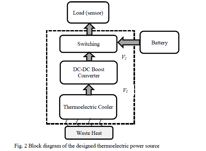
| A block diagram of the proposed thermoelectric power source is shown in Fig. 2. It uses waste heat. It consists of three main parts: a TEC for converting thermal energy into electrical power; a small-input voltage DC-DC boost converter to step up the generated TEC voltage V1and a switching Schottky diode (IN5817) for automatically selecting power supply between the proposed TEC power source and battery. The TEC chosen in the proposed thermoelectric power source by HB Corporation with dimensions of 40mm x 40mm x 3.8mm can be operated from -30°C to 138°C. |
 |
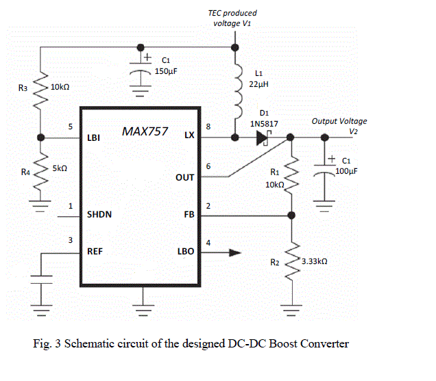
| A DC-DC converter is designed to step up the produced voltage V1 of the TEC using MAX757 shown in Fig. 3. This circuit can boost voltage V1 down to 0.7 to higher output voltage V2in the range from 2.7V to 5.5V. The output voltage V2is set by two network resistor R1 and R2. This forms a voltage divider between the output and the FB pin with VREF = 1.25V as shown in Fig. 3. Output voltage, Vout can be determined by: |
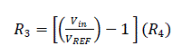
| Since the input bias current at FB has a maximum current of 100nA, large valuesfor R1 and R2can be chosen and in this designed circuit, R1 = 10kΩ and R2 = 3.33kΩ. The MAX757 contains on-chip circuitry for low battery detection. If the voltageat Low Battery Input (LBI) falls below the regulator’s internal reference voltage(1.25V), Low Battery Output (LBO) which is an open drain output sinks current to GND. Thelow-battery monitor's threshold is set by two resistors, R3 and R4 whichforms a voltage divider between the input voltage and the LBI pin. The threshold voltageis set by R3 and R4. The two resistances used in this designed circuit are 10kΩ and 5kΩ, respectively and the following equation is used to determine the values: |
 (2) (2) |
| Inductor selection has also been considered in this design. The inductor should have a saturation current rating equal to or greater than the peak switch current limit which is 1.2A. The 22μH inductor has been used in this design because of its capability in the typical MAX757 applications circuits. A Schottky diode 1N5817 is used for optimum performance as shown in Fig. 3. The diode offers low switching noise, low forward voltage drop, high current capability, high switching capability, high reliability and high surge capability. |
 |
III.EXPERIMENTAL RESULT |
| A. Current –Voltage Characteristic and Maximum Power Tracking of TEC |
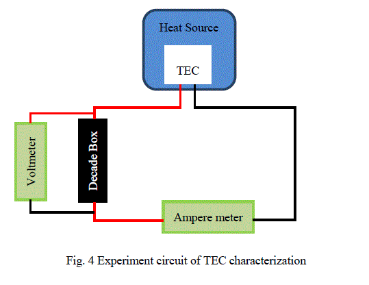
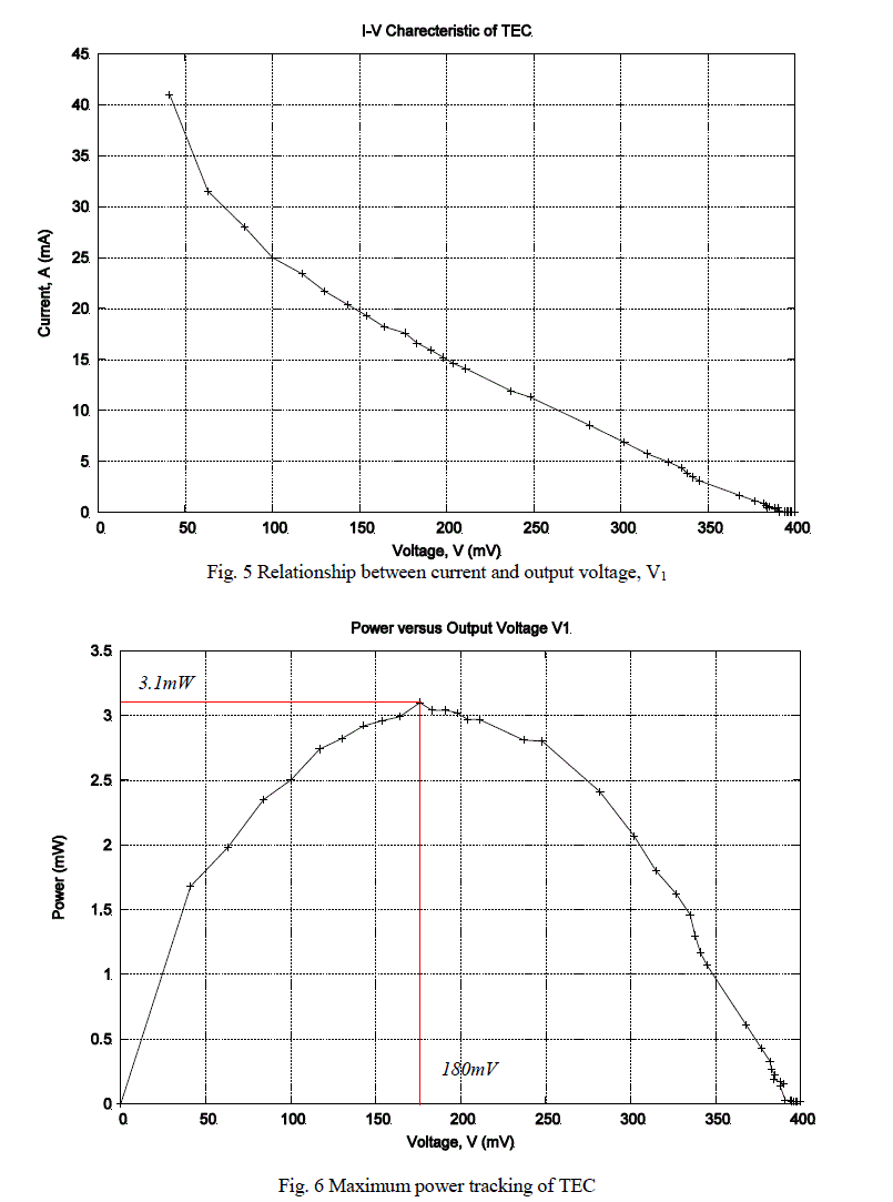
| The characterization of TEC module was performed by setting the temperature at 100°C from thermal source which was connected in serries with decade box resistor as shown in Fig. 4. The value of decade box resistor was varied from 10kΩ to 1Ω. Then, current and output voltage V1 produced by TEC for each varied resistor values were measured. In this experiment, a high input resistance voltmeter was used to minimize the load effect. Fig. 5 shows the relationship between current and output voltage V1 which is the current inversely proportional to the output voltage V1. The graph also shows that the produced currents and voltages were very low. This is not sufficient to be a source voltage if the circuit uses only passive components. However, by using this designed DC-DC Boost converter, the small voltage produced is able to be boosted. |
 |
 |
| B. Measured Results of the designed DC-DC boost converter |
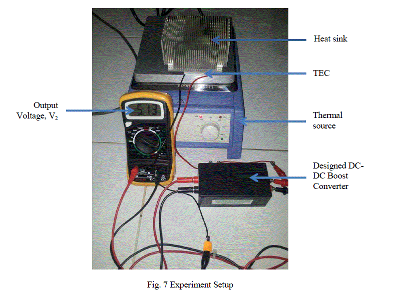
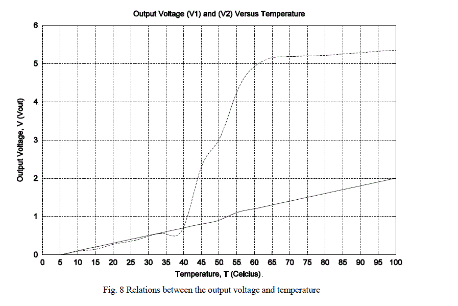
| To evaluate the performance of the designed DC-DC boost converter, a series of measurement was performed using the circuit shown in Fig. 7. The input of DC-DC boost converter was connected to the TEC module and the output of DCDC boost converter was connected to a high input resistance voltmeter to measure output voltage V2. The TEC module was sandwiched between thermal source surface (TEC hot side) and heat sink (TEC cold side). The heat sink was attached on the cold side in order to maintain the low temperature and produce higher voltage. Temperature from thermal source was varied and the produced output voltage V1 and V2 were recoded as shown in Fig. 8. |
 |
| Fig. 8 shows the relationship between both output voltages and temperature. The graph illustrates the number of temperature in °C that was set to evaluate the performance of the designed DC-DC boost converter from 5°C to 100°C. Both output voltages V1 and V2 are proportional to the temperatures. At temperature between 5°C to 40°C, the input voltage V1 was not stepped up by the converter and equal to output voltage V2 because V1 was lower than 0.7V which is minimum required input voltage for the designed DC-DC boost converter. As the temperature increased above 40°C, the output voltage V1 also increases. The designed DC-DC boost converter was able to boost the voltage V1 and the output voltage V2 increased sharply until the temperature equals to 65°C. At 65°C, the output voltage V1 and V2 were 1.4V and 5.2V, respectively. The consistent rise was seen in the output voltage V1 when the temperature keeps increasing until 100°C but the output voltage V2seems to saturate in the range 5.2 to 5.4V which is the maximum produced voltage of the designed DC-DC boost converter. |
 |
IV.CONCLUSION |
| The Seebeck effect-based thermoelectric power source using TEC module has been presented in this paper. One great advantage of the designed concept is that the TEC energy harvester is employed to recover waste heat in industrial process as a renewable energy source and green technology. Experimental results confirm that the designed DC-DC boost converter is able to produce the desired output voltage for powering other electronic circuit. A stage of DC-DC boost converter can be connected to the designed DC-DC boost converter if higher output voltage is required. |
ACKNOWLEDGMENT |
| The authors are grateful to UniversitiTeknikal Malaysia Melaka because this work is financially supported by the university under PJP grant scheme (No: PJP/2012/FKEKK(39A)/S01043). |
References |
|