Keywords
|
| DCVS logic, Low Power, Delay |
INTRODUCTION
|
| Comparator plays an important role in high speed analog to digital converters. A comparator is a device, which compares two analog signal or voltages and produce the digital output based on the comparison. Comparators are also called as 1-bit analog to digital converter, for that reason they are mostly used in large quantity in A/D converter. A clocked comparator generally consists of two stages. In that first stage is to interface the input signals. The second (regenerative) stage consists of two cross coupled inverters, where each input is connected to the output of the other. In the double tail comparator power consumption is quite high due to delay. It can be reduced by adding switching transistors and using DCVS logic design. The proposed comparator based on DCVS logic. Here by using two pull down networks the power consumption going to reduce. It has many advantages compared to the CMOS logic. It has reduced circuit delay and increased speed of action and reduces layout density and power dissipation .The DCVS logic has extended logic flexibility. The speed of the comparator is justified based on the delay time. In many low power applications comparator speed, power dissipation, offset voltage, supply voltage, power efficiency and number of transistors are more important. By using DCVS logic to design the comparator, power dissipation and delay time is reduced. It is a static logic which consumes no dynamic power. It uses latch to compute the output quickly. It uses a latch structure in the pullup side which eliminates static power consumption and provides true and complement outputs. |
RELATED WORKS
|
| In [2] author presents successive approximation analog to digital converter designed based on supply boosting technique to reduce the power and voltage of the circuits. In[3] authors reduce voltage of the mixed signal circuits by using supply boosting technique(SBT) and it can be used if very low power analog signal processing operations are performed on continuous or discrete time signals. In[4] author used body driving technique to reduce the power and voltage of mixed signal design. In[5] author introduce sub-1v modulator with 1-bit quantiser with rail to rail input range. In[6] authors used bandwidth modulation technique to design clocked comparator for increasing the speed of the circuit. In[7] comparator designed by using 0.12 μm CMOS technology and operating with 1.5v at 6GHz. In[8] comparator designed by using 65nm CMOS technology with modified latch to reduce supply voltage. |
EXISTING DESIGN
|
| A. Conventional Dynamic Comparator: |
| This comparator widely used in A/D converters, relaxation oscillator, and null detector with high input impedance, rail-to-rail output swing and no static power consumption. These comparators are clocked and they produce output after the transition of the clock. The value of the input to a clocked comparator is only of concern in a short time interval around the clock transition. The modes of operation depend on the clock input given. CLK= 0 is called reset phase and CLK = Vdd is called as evaluation phase. When CLK = 0, nMOS transistor is off and pMOS transistor is on. When CLK = Vdd, nMOS is on and pMOS transistor is off. The speed of this comparators is very high and the power dissipation of this comparators can be very low .The comparators using clock signals are called dynamic Comparators. Regenerative feedback is often used in dynamic comparators and also in non-clocked comparators. |
| The operation of the comparator is explained below. During the reset phase when CLK = 0 the Mtail is in off, reset transistors (M7– M8) pull both output nodes Outn and Outp to VDD to define a start condition and to have a valid logical level during reset. After when CLK = VDD, transistors M7 and M8 are off, and Mtail is on. Output voltages (Outp, Outn), are pre-charged to VDD, then started to discharge with different discharging rates depending on the input voltage (INN/INP) given to the comparator. Now consider this case where VINP > VINN, then the Outp discharges faster than Outn, hence when Outp (discharged by transistor M2 drain current), falls down to VDD–|Vthp| before Outn (discharged by transistor M1 drain current), the corresponding PMOS transistor (M5) will turn on in the latch regeneration caused by back-to-back inverters and M4, M6). Thus Outn goes to VDD and Outp discharges to ground. If VINP < VINN, the circuits operate inversely. |
| B. Conventional Double Tail Comparator: |
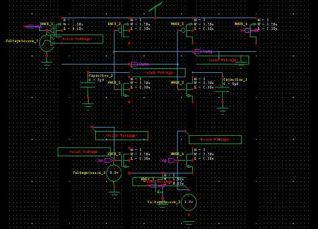
| Double tail comparator is used in low power applications. In this method, increase the voltage difference between the output nodes in order to increase the latch regeneration speed. For this purpose, two control transistors has been added to the first stage in parallel to M3 and M4 transistors in a cross- coupled manner. Double tail comparator has two operation modes, the reset phase and another one is decision making phase. The double tail enables both a large current in the latching stage and in Mtail2, for fast latching independent of the input commonmode voltage (Vcm), and a small current in the input stage (small Mtail1), for low offset . During reset phase (CLK = 0, Mtail1, and Mtail2 are off), transistors M3-M4 pre-charge fn and fp nodes to VDD, which makes transistors MR1 and MR2 to discharge the output(outn,outp) nodes to ground. |
| C. Double tail dynamic comparator : |
| In this type of comparator without complicating the design and by adding few transistors, the positive feedback during the regeneration is strengthened, which results in reduced delay time. During reset phase (CLK=0 Mtail1 and Mtail2 are off avoiding static power),M3 and M4 pulls both fn and fp nodes to VDD hence Mc1 and Mc2 are in cut off .Intermediate stage transistor MR1 and MR2reset both latch outputs to ground. During decision making phase (CLK=VDD Mtail1, and Mtail2 are on), transistors M3 and M4 turn off. Furthermore, at the beginning of this phase, the control transistors are still off (since fn and fp are about VDD). Thus, fn and fp start to drop with different rates according to the input voltages. Suppose VINP >VINN, thus fn drops faster than fp, (since M2 provides more current than M1). As long as fn continues falling, the corresponding PMOS control transistor (Mc1 in this case) starts to turn on, pulling fp node back to the VDD; so another control transistor (Mc2) remains off, allowing fn to be discharged completely. One of the points which should be considered in this circuit, when one of the control transistors (e.g.,Mc1) turns on, a current from VDD is drawn to the ground via input and tail transistor (e.g., Mc1, M1, andMtail1) resulting in static power consumption. To overcome this problem, two NMOS switches are used below the input transistor. |
| Thus the average power consumption of the double tail dynamic comparator is 12μW and the delay is 7.4ns. Compared with the conventional double tail dynamic comparator it has less power and delay. |
PROPOSED DESIGN
|
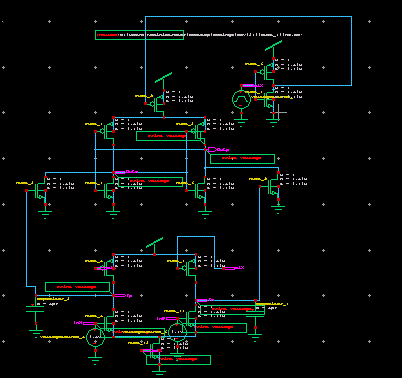
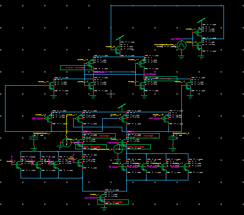
| The Differential Cascode Voltage Switch (DCVS) logic is the the most widely used structure to design CMOS circuits due to the advantages over traditional NAND/NOR circuit techniques. Differential Cascode Voltage Switch (DCVS) logic is a CMOS circuit design technique with numerous advantages over the conventional static CMOS. It is a static logic which consumes no dynamic power. It uses latch structure to compute output quickly. It uses a latch structure for the pullup which eliminates static power consumption and provides true and complement outputs. |
| Depending up on the state of differential inputs, the two nodes connecting pullup and pull down network get pull down by one of the Nmos logic tree. The regenerative action of PMOS maintain the outputs outn and outp to be static and obtains full voltage swing Vdd or ground of its outputs. |
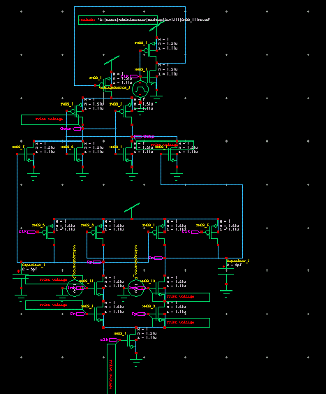
| During the reset phase when CLK = 0 and Mtail is off, reset transistors (M7– M8) pull both output nodes Outn and Outp to VDD to define a start condition and to have a valid logical level during reset. |
| During decision-making phase (CLK = VDD, Mtail1 and Mtail2 turn on), M3-M4 turn off and voltages at nodes fn and fp start to drop with the different rate dependent differential voltage. VINP >VINN, thus fn drops faster than fp, (since M2 provides more current than M1). As long as fn continues falling, the corresponding PMOS control transistor (Mc1 in this case) starts to turn on, pulling fp node back to the VDD; so another control transistor (Mc2) remains off, allowing fn to be discharged. In this design by adding more number of switching transistors the delay time can be reduced. Based on the input voltage, output started to drop at different rates. |
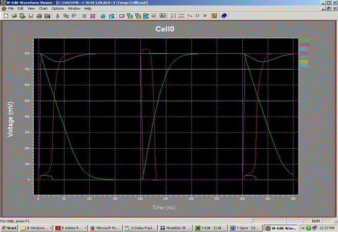
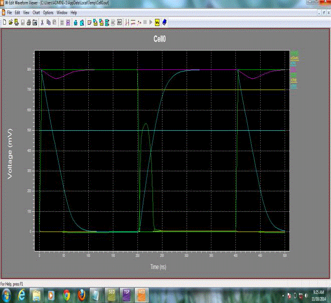
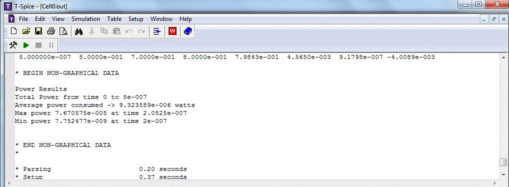
| If the input voltage given to the comparators are INN is 0.7v and INP is 0.5v, so that outn discharge faster than outp. Thus the simulated output shown in fig.6.The power consumption of this comparator is 9.3μw is calculated by using T-SPICE tool. |
CONCLUSION
|
| Power and delay estimation is calculated by using post layout simulation with the help of Tanner EDA tools. In order to compare the DCVS logic based comparator with the single tail comparator , the conventional double tail comparators and double tail comparator, all circuits have been simulated in 180 nm CMOS technology, VDD = 0.8v.Thus the power consumption DCVS logic based comparator is is less than double tail comparator and delay also reduced. |
Tables at a glance
|
 |
| Table 1 |
|
Figures at a glance
|
 |
 |
 |
 |
| Figure 1 |
Figure 2 |
Figure 3 |
Figure 4 |
|
 |
 |
 |
| Figure 5 |
Figure 6 |
Figure 7 |
|
References
|
- SamanehBabayan, Mashhadi and Reza Lot fi, "Analysis and Design of a Low-Voltage Low-Power Double Tail Comparator”,pp.1-10 , 2013.
- S. U. Ay, “A sub-1 volt 10-bit supply boosted SAR ADC Design in standard CMOS,” Int. J. Analog Integr. Circuits Signal Process., vol. 66 no.2, pp.213–221, 2011.
- A.Mesgarani, M. N. Alam, F. Z. Nelson, and S. U. Ay, “Supply boosting technique for designing very low voltage mixed-signal circuit instandard CMOS,” in Procce. IEEE Int. Midwest Symp. Circuits Syst.Dig.Techni Papers, pp. 893–896,2010.
- B.J. Blalock, “Body-driving as a Low-Voltage Analog Design Technique for CMOS technology,”.IEEE Southwest Symp. Mixed-SignalDesign, pp 113–118,2000.
- M. Maymandi-Nejad and M. Sachdev, “1-bit quantiser with rail to rail input range for sub-1V modulators,” IEEE Electron, vol. 39, no.12, pp.894–895, 2003.
- Y. Okaniwa, H. Tamura, M. Kibune, D. Yamazaki, T.-S.Cheung,J.Ogawa, N. Tzartzanis, W. W. Walker, and T. Kuroda, “A 40Gb/ s CMOSClocked comparator with bandwidth modulation technique,” IEEE J. Solid-State Circuits, vol. 40, no. 8, pp. 1680–1687, 2005.
- B. Goll and H. Zimmermann, “A 0.12 μm CMOS Comparator requiring 0.5V at 600MHz and 1.5V at 6 GHz,” in Proc. IEEE Int. Solid-State Circuits Conf., pp. 316–317,2007.
- B. Goll and H. Zimmermann, “A 65nm CMOS comparator with modified latch to achieve 7GHz/1.3mW at 1.2V and 700MHz/47μW at0.6V,” in Proc. IEEE Int. Solid-State Circuits Conf, pp. 328–329,2000
|