International Journal of Advanced Research in Electrical, Electronics and Instrumentation Engineering
ISSN ONLINE(2278-8875) PRINT (2320-3765)
ISSN ONLINE(2278-8875) PRINT (2320-3765)
| 1Naveen L J, 2 Vinutha C B, 3Abdul Imran Rashid, 4Dr. M Z Kurian |
| Related article at Pubmed, Scholar Google |
Visit for more related articles at International Journal of Advanced Research in Electrical, Electronics and Instrumentation Engineering
In digital communication Orthogonal Frequency Division Multiplexing (OFDM) is regarded as a promising technology in recent years. In this paper, propose low power transceiver for OFDM based wireless local area network (WLAN) system using Application Specific Integrated Circuit (ASIC) platform. As per the IEEE standard 802.11a OFDM based transceiver are capable of providing data rates up to tens of Mbps but OFDM transceiver will dissipate huge amount of power. The objective of the work is the optimization with respect to power & area. It includes various low power libraries as well as ample amount of low power constrain
Keywords |
| OFDM, WLAN, ASIC, low power transceiver, IEEE 802.11a |
INTRODUCTION |
| Orthogonal frequency division multiplexing (OFDM) is a special case of multicarrier transmission, where a single data stream is transmitted over a number of lower rate subcarriers. OFDM can be seen as either a modulation technique or a multiplexing technique [1] |
| One of the main reasons to use OFDM is to increase the robustness against frequency selective fading or narrowband interference. In a single carrier system, a single fade or interferer can cause the entire link to fail, but in a multicarrier system, only a small percentage of the subcarriers will be affected. Error correction coding can then be used to correct for the few erroneous subcarriers [1], [2] |
II. LITEARTURE SURVEY |
(a). Orthogonal Frequency Division Multiplexing.(OFDM) |
| Orthogonal Frequency Division Multiplexing (OFDM) is one of the Multi-Carrier Modulation (MCM) techniques that transmit signals through multiple carriers. These carriers (subcarriers) have different frequencies and they are orthogonal to each other. Orthogonal frequency division multiplexing techniques have been applied in both wired and wireless communications, such as the IEEE 802.11a standard [1], [2]. |
(b). Orthogonality. |
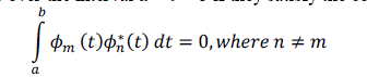
| Orthogonality is defined for both real and complex valued functions. The functions φm(t) and(φn(t) are said to be orthogonal with respect to each other over the interval a < t < b if they satisfy the condition. |
 |
| OFDM splits the available bandwidth into many narrowband channels (typically 100-8000), each with its own subcarrier. These sub-carriers are made orthogonal to one another, meaning that each one has an integer number of cycles over a symbol period. Thus the spectrum of each sub-carrier has a “null” at the centre frequency of each of the other sub-carriers in the system, as demonstrated in Figure 2.1. This results in no interference between the sub-carriers, allowing them to be spaced as close as theoretically possible. Because of this, there is no great need for users of the channels to be time-multiplexed, and there is no overhead associated with switching between users. This overcomes the problem of overhead carrier spacing required in FDMA [1], [2], [3]. |
III. LOW POWER AT DIFFERENT LEVELS OF VLSI DESIGN |
| Low power chip requirement in the VLSI industry is main considerable field due to the reduction of chip dimension day by day and environmental factors. [4] |
| Low Power Design Methodologies presents the first in-depth coverage of all the layers of the design hierarchy, ranging from the system layer, architectural levels, logic and circuit, up to the technology.[4] |
(a) System Level |
| A system typically consists of both hardware and software components, which affect the power consumption. The system design includes the hardware/software partitioning, hardware platform selection (application-specific or general purpose processors), resource sharing (scheduling) strategy, etc. The system design usually has the largest impact on the power consumption and hence the low power techniques applied at this level have the most potential for power reduction.[4],[7]. |
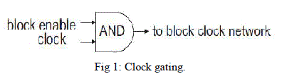
| The power-down and clock gating are two of the most used low power techniques at system level. The non-active hardware units are shut down to save the power. The clock drivers, which often consume 30-40% of the total power consumption, can be gated to reduce the switching activities as illustrated in Fig 1 |
 |
| (b) Algorithm Level |
| The algorithm selections have large impact on the power consumption. For example, using fast Fourier transform instead of direct computation of the DFT reduces the number of operations with a factor of 8 for an 8-point Fourier transform and the power consumption is likely to be reduced with a similar factor. The task of algorithm design is to select the most energy efficient algorithm that just satisfies the constraints. The cost of an algorithm includes the computation part and the communication/storage part. The complexity measurement for an algorithm includes the number of operations and the cost of communication/storage. Reduction of the number of operations, cost per operation, and long distance communications are key issues to algorithm selection |
| One important technique for low power of the algorithmic level is algorithmic transformations. This technique exploits the complexity, concurrency, regularity, and locality of an algorithm .Reducing the complexity of an algorithm reduces the number of operations and hence the power consumption. The possibility of increasing concurrency in an algorithm allows the use of other techniques, e.g., voltage scaling, to reduce the power consumption. The regularity and locality of an algorithm affects the controls and communications in the hardware [6], [8]. |
| (c) Architecture Level |
| The implementation dependent part of the power consumption of a system is strongly related to a number of properties that a given system or algorithm. The component that contributes a significant amount of the total energy consumption is the interconnect. The power consumption of the interconnect is highly dependent on algorithm and architecture-level design decisions. Two properties of algorithms are important for reducing interconnect power consumption are locality and regularity [6]. |
| Locality relates to the degree to which a system or algorithm has natural isolated clusters of operation or storage with a few interconnections between them. Partitioning the system or algorithm into spatially local clusters ensures that the majority of the data transfers take place within the clusters and relatively few between clusters. The result is that the local buses are shorter and more frequently used than the longer highly capacitive global buses. Regularity in an algorithm refers to the repeated occurrence of computational patterns. Common patterns enable the design of less complex architecture and therefore simpler interconnect structure (buses, multiplexers, buffers) and less control hardware. |
| As the algorithm is selected, the architecture can be determined for the given algorithm. As it can see from Eq. (2.16), an efficient way to reduce the dynamic power consumption is the voltage scaling. When supply voltage is reduced, the power consumption is reduced. However, this increases the gate delay. The delay of min-size inverter (0.35 mm standard CMOS technology) increases as the supply voltage is reduced. [6] [8]. |
| (d) Logic Level |
| The power consumption depends on the switching activity factor, which in turn depends on the statistical characteristics of data. However, most low power techniques do not concentrate on this issue from the system level to the architecture level. The low power techniques at the logic level, however, focus mainly on the reduction of switching activity factor by using the signal correlation and, of course, the node capacitances [6], [9]. |
| (e) Circuit Level |
| At the circuit level, the potentials power saving are often less than that of higher abstract levels. However, this cannot be ignored. The power savings can be significant as the basic cells are frequently used. A few percents improvement for D flip-flop can significantly reduce the power consumption in deep pipelined systems [9]. |
| In CMOS circuits, the dynamic power consumption is caused by the transitions. Spurious transitions typically consume between 10% and 40% of the switching activity power in the typical combinational logic. In some cases, like array multipliers, the amount of spurious transitions is large. To reduce the spurious transitions, the delays of signals from registers that converge at a gate should be roughly equal. This can be done by insertions of buffers and device sizing. The insertions of buffer increase the total load capacitance but can still reduce the spurious transitions. This technique is called path balancing [6], [9] |
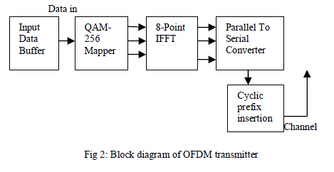 |
| Fig 2 shows the simplified block diagram of OFDM transmitter. The generation of OFDM signal started from amplitude modulation mapping bank. The serial input data is mapped to appropriate symbol to represent the data bits. These symbols are in serial and need to convert into parallel format since IFFT module requires parallel input to process data. The serial to parallel module does the conversion. These parallel symbols are transformed from frequency domain into time domain using IFFT module. These signals are converted into serial format and add a cyclic prefix to data frame before being transmitted. |
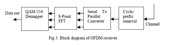 |
| Fig 3 shows the basic block diagram for receiver module. There are five modules in the receiver block and initially the cyclic prefix has to be removed from the received signals. As the received data is in serial format, and since FFT requires input in parallel format, a module which converts serial data to parallel data is required. Output from FFT is converted back to serial format through parallel to serial converter. The conversion is required since the serial data need to be transmitted. Finally the serial output is demodulated using de-mapping module to get the transmitted data. |
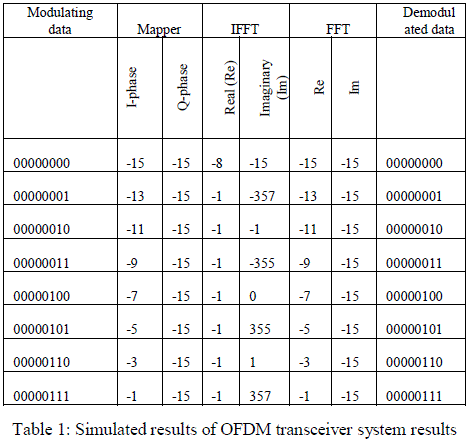
| All these modules are designed using the verilog coding, once the code is ready and simulated using the Xilinx software or using synopsys verilog compiler simulator in ASIC. OFDM system results are synthesized and simulated using ASIC platform.Table1 shows the complete operation at every modules of transmitter and receiver of the OFDM system. |
 |
LOW POWER TRANSCEIVER FOR OFDM |
| Now the all the OFDM module is synthesized and simulated and now we are applying various low power constraints to these codes we get area and power report. In our work we apply two low power constraints as worst case and best case. After that we apply clock gating low power technique to this design to reduce the power. On applying “tcbn65lphvtbc_140” as technology library to OFDM module, properly synthesized and mapped to get the area and power report as given in below Table 2. |
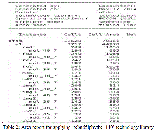 |
| Table 2 shows the area report of OFDM when applying “tcbn65lphvtbc_140” as technology library. It gives the cell area of OFDM as 70361 microns and consumes 12528 cells. Similarly on the same library we get power report as shown in table 3. |
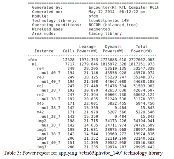 |
| This report yields the total power consumption of OFDM module as 2727062.9(nw) of power with the loss of 1974.3(nw) of leakage power and 2725058(nw) of dynamic power. This is the worst case scenario where the above area and power reports show that the design consumes larger area and maximum power respectively. Therefore we apply one more low power constraint to OFDM module, the results of which are shown in Table 4 and Table 5. |
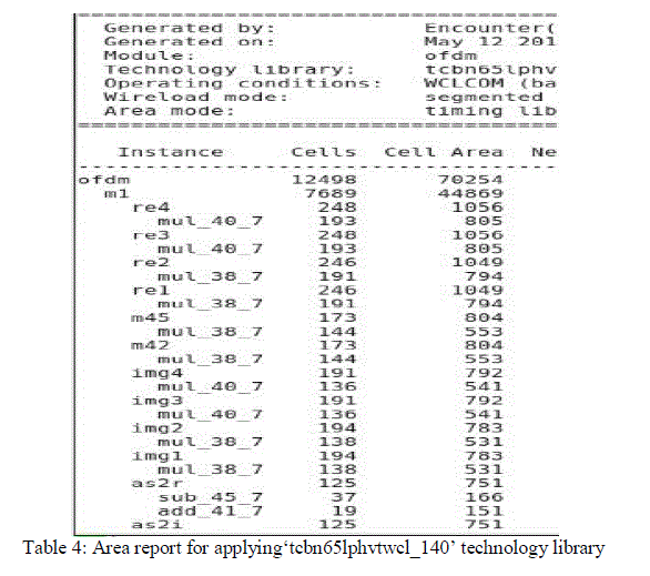 |
| Here “tcbn65lpvtwcl_140” technology library were applied the area report is shown in table 4. In this case OFDM module consumes 70254 microns cell area and consumes 12498 cells. |
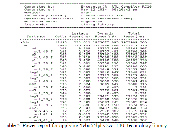 |
| Table 5 shows the power report for applying ‘tcbn65lphvtwc_140’ technology library and it consumes 1973909.5(nw) total power with the loss of 19733677.8(nw) dynamic power and 231.6(nw) leakage power. By comparing the above constraints with results, “tcbn65lpvtwcl_140” is best case scenario because it consumes less power and less area as compared to “tcbn65lphvtbc_140” technology library. |
| From the above experiment, the following inference is obtained that “tcbn65lpvtwcl_140” is best case technology library but the power can still be reduced to higher extent by applying clock gating technique to this library then the following results in Table 6 and Table 7 will be obtained. |
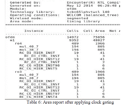 |
| After applying the clock gating to the best case library it yields the area report as shown in table 6 here it consume 75856 cell area in terms of microns, and consumes 14972 cells. |
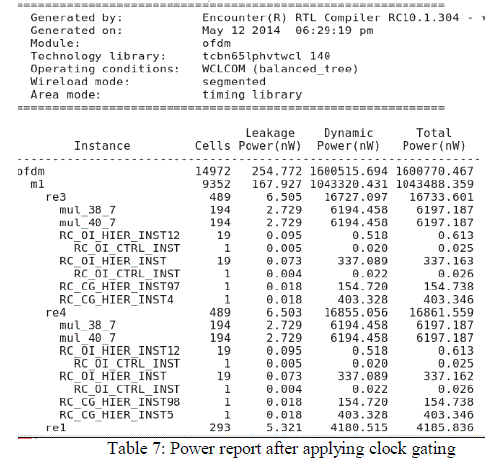 |
| After applying the clock gating to the best case library it yields the power as 1600770.4(nw) of total power consumption and dynamic power as 1600515.6(nw). By comparing the best case scenario with the clock gating technique, it is seen that less power is utilized. However, it consumes more cell area and cells because in this technology extra AND gates are inserted into the OFDM modules to reduce the switching power consumption. Therefore, obliviously area will be relatively increased. |
V. CONCLUSION |
| In this paper, the Low power transceiver for OFDM based WLAN system on ASIC platform is presented by using ample number of various low power libraries. It can be observed that comparing each library, the best case for implementation in real time can be selected. From the above experiment and results we conclude that clock gating reduces power consumption further. So power and area is always the traded-off between one another, depending on the requirement any one case can be selected for real time implementations. Further, many more low power libraries are there to reduce the power, area, as well as timing to yields the better performance. |
References |
|