International Journal of Advanced Research in Electrical, Electronics and Instrumentation Engineering
ISSN ONLINE(2278-8875) PRINT (2320-3765)
ISSN ONLINE(2278-8875) PRINT (2320-3765)
R.Rajith, S.Selva Prabhu
|
| Related article at Pubmed, Scholar Google |
Visit for more related articles at International Journal of Advanced Research in Electrical, Electronics and Instrumentation Engineering
In this paper, we discuss logic circuit designs using the circuit model of three-state quantum dot gate field effect transistors (QDGFETs). QDGFETs produce one intermediate state between the two normal stable ON and OFF states due to a change in the threshold voltage over this range. We have developed circuit model which has intermediate state. Various logic can be implemented using QDGFETs. In this paper, we have discussed the designs of various three-state QDGFET combinational circuits like decoder, and comparator. Increased number of states in three-state QDGFETs will increase the number of bit-handling capability of this device and will help us to handle more number of bits at a time with less circuit elements.
Keywords |
| QDGFET, ternary logic,field effect transistor, MVL, |
I. INTRODUCTION |
| Binary logic has been used for electronic designs for many decades. The challenges of the binary logic have inspired the researchers for research in multi-valued logic (MVL). For example, with binary logic designs, chip interconnects occupy so much area that it limits the performance of the VLSI chips [1]. Binary algebra also takes more digits to represents any number when compared to any higher radix algebra [2]. Going to Multi valued logic may have some efficient solutions for these challenges. Use of multi value logic ternary logic for interconnect is definitely a good way to reduce the data related metal interconnect density to half. In addition ternary logic algebra inherently processes the information for efficiently and reduced the number of transistors required to compute a calculation when compare to processing in binary logic. In ternary logic the levels are represented by 0, 1, 2, . Significant research have been done on multi valued logic and quaternary logic in past few decades [1,2]. Researchers have explored the suitable algebra for logic and arithmetic, optimized the logic algorithms, and developed the test algorithms for multi valued logic. Though so much work has been put into research we still do not see much of implementations in MVL. One of the reasons for this is availability of suitable transistors to implement all these logic and arithmetic functions offered by the MVL research. |
| MVL can be implemented using different kinds of devices like resonant tunneling diodes [3], [4], resonant tunneling transistors [5]–[7], modulation-doped FETs [8]– [10], high electron mobility transistors [11]–[13], carbon nanotube field effect transistors (CNTFETs), single electron transistors (SETs), and so on. Among these semiconductor devices, CNTFET and SET are the most promising devices to implement the MVL in future. |
| In the CNTFET-based ternary logic circuits [14], the circuit design is based on different CNTFETs which have different threshold voltages based on the CNTs diameter thickness. Ternary logic architecture based on CNTFET is different than the conventional CMOS architecture. In the resistor-based CNTFET circuits, the value of the resistor is so high that it is difficult to fabricate. On the other hand, the conventional CNTFET-based circuit has more number of elements than that in the CMOS circuit, for example, standard ternary inverter (STI) has six CNTFETs. Besides this uniform CNTs having same diameter and similar orientation are difficult to fabricate. |
| On the other hand, the main problems of SET-based [15] logic implementation is lithography techniques, background charge, co-tunneling, and room temperature operation. Two major drawbacks of the SET as an electronic circuit component are, it does not have internal memory and it cannot carry DC, so that an ultrasensitive electrometer is necessary to measure its charge state |
| Exact copying of CMOS circuits using SET is impossible, and in order to get substantial parameter margins, even the simplest logic gates have to be redesigned. Besides this, their operation range starts shrinking under the effect of thermal fluctuations as soon as their scale kBT reaches approximately 0.01E |
| Because of the presence of quantum dots in the gate region, QDGFET produces one intermediate state between its two stable states in its transfer characteristics [16], [17]. The generation of the intermediate state can be explained by the resonant tunneling of charge carriers from the inversion channel to the quantum dots on top of the gate region. Since the quantum dots in the gate region are cladded by a high band gap insulator, charge leakage for these devices are very small, which provides the stability to the generation of the intermediate state between its normal ON and OFF states. Another advantage of QDGFET is that it can be fabricated in conventional CMOS process at room temperature. The quantum dot self-assembly is also performed at room temperature. The threshold voltage of QDGFET can be controlled easily either by varying the gate insulator thickness or varying the number of quantum dot layers on top of the gate region. The background charge problem of SET is also absent in QDGFET. |
| In our proposed circuit design, we use QDGFET as the key circuit element which itself can produce three states in its transfer characteristics. QDGFETs can be used in the conventional CMOS architecture to implement ternary logic circuits. The design complexity will decrease when implementing ternary logic circuits based on QDGFET. |
| This paper is organized as follows. Section II describes about the structure of QDGFET. Sections III and IV highlight on the theory of operation and circuit model. The inversion operation, ternary logic decoder and 1 bit ternary compatator are discussed in Sections V, VI, and VII, respectively, which is followed by the conclusions in Section VIII |
II.QUANTUM DOT GATE FIELD EFFECT TRANSISTOR |
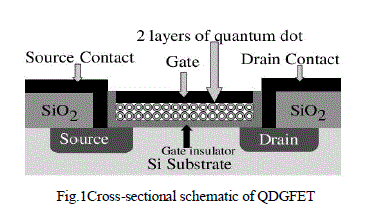
| A quantum-dot gate (QDG) field-effect transistor (FET), exhibiting 3-state transfer characteristics, differs from a conventional FET as well as floating gate nanodot nonvolatile memories in its gate structure. In QDG-FETs, two or more layers of SiOx cladded Si quantum dot (or GeOx cladded Ge) quantum dots are self-assembled (as shown in Figure 1a) on top of a thin gate insulator [20, 21]. Source and drain regions are formed in quantum dot gate field effect transistor like a conventional FET. The gate tunnel insulator layer could be SiO2 or HfO2 or a lattice-matched epitaxial layer of high-κ dielectric. Unlike floating gate QD nonvolatile memories [22-23] where the charge is permanently stored in the quantum dot layer, a three-state QDG-FET device does not have a thick outer control gate insulator layer and the charge is permitted to escape the dot via tunneling through a very thin (~1nm) SiO2 cladding layer around the Si. In addition, QDGFETs have at least two cladded quantum dot layers separated by a thin barrier that permits tunneling of electrons. It was observed that QDG-FET structures without an outer control gate insulator (such as nitride layer) exhibit the three-state behavior. |
| Because of the presence of quantum dots in the gate region, QDGFET produces one intermediatestate “i” between its two stable states in its transfer characteristics. The occurrence of “i” state is explained by the transfer of the channel electrons (as a function of the gate voltage) to one of the two quantum dot layers which in turn increases the threshold voltage. An increase in the gate voltage VG is thus compensated by an increase in the threshold voltage VTH, thereby keeping ID nearly constant. The range of gate voltage over which ‘i’ behavior is observed is determined by the resonant tunneling across two layers of quantum dots and the rate of electron transfer from inversion channel to dots.Fig. 1(a) shows the crosssectional schematic of a QDGFET. |
III.THEORY OF OPERATIONS |
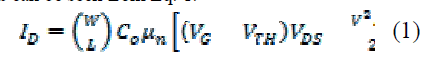
| In a conventional FET, the threshold voltage does not vary appreciably during operation and ID increases with VG as can be seen from Eq. 1. |
 |
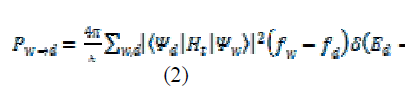
| However, in a QDG-FET, an increase in the gate voltage is accompanied by an increase in the threshold voltage. This causes slow or no increase in the drain current, as the (VG - VTH) term remains constant. In other words, increases in gate voltage are compensated by increases in the threshold voltage, and the drain current either does not increase at all or increases very slightly. This results in the manifestation of an intermediate state ‘i’ where the drain current virtually remains constant. The range of gate voltage in which this occurs depends on: (1) the relative location of the quantum dot energy levels with respect to the energy levels of the quantum well inversion channel, and (2) the rate of charge transfer from channel to QD layers.The tunneling probability can be expressed as [18, (2)] |
 |
| The charge in the gate region due to quantum dots is discrete as expressed by Eq. 3.The variation in flat band voltage VFB due to the charged state of quantum dots in the gate results in corresponding change in the threshold voltage ΔVTH. The variation in the value of charge on the two QD layers, as the Vg is increases, causes changes in the threshold voltage expressed in Eq. 3. |
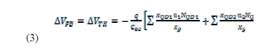 |
| Here, xQD1and xQD2 are the distances of quantum dot cores from the gate contact, n1 and n2 are the number of dots in layer 1 and 2, respectively, NQD1 and NQD2 are the charge on each SiOx-cladded Si quantum dots, Cox is the oxide capacitance (which is modified due to the presence of quantum dots). In addition, xg is the distance of the Si- SiO2 interface from the gate, ρ is the charge density and q is the electron charge. |
IV. QDGFET CIRCUIT MODEL |
 |
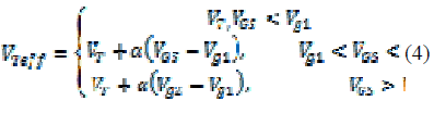
| The effective threshold voltage is divided into three regions, OFF state, intermediate state and ON state, corresponding to the fabricated device transfer characteristics. The threshold voltage of a QDGFET can be expressed according to (4). |
| As the gate voltage increases, initially the threshold voltage is same as a conventional FET which is represented by VT. When the gate voltage increases through a range of voltages, (Vg1 to Vg2), the threshold voltage changes linearly with respect to the gate voltage. This changes is controlled by the α parameter. With α= 0, the model behaves like a conventional FET and with α= 1 the model has a threshold voltage that changes directly with the gate voltage which represents QDG-FET characteristics. The parameter α depends on the size and number of dots which can be controlled at fabrication time, and as a result change the QD gate charge. The Vg1 and Vg2 terms are also determined at fabrication time. Using the equations for VTeff from Eq.(4), the drain current equations can be derived using traditional MOSFET circuit modeling techniques |
 |
 |
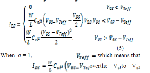 |
| region. According to this equation,IDS is independent ofVGSover thisregion, leading to a flat current curve over the region. Using these principles, the Vthof conventional FET is modified according to (4) in Berkeley Simulation model (BSIM 3.2.0 and BSIM 3.2.4) which is very popular for nano-FET modeling and conducted simulations of QDG-FET based ternary logiccircuits using Cadence. |
V. THREE STATE COMPLEMENT FUNCTION |
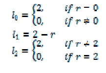
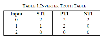
| A ternary inversion is an operation with one input (r)and three outputs (l0, l1,and l2) such that where r is the number of states in the logic space [18]. The implementation of ternary inverters requires three inverters: negative ternary inverter (NTI), STI, and positive ternary inverter (PTI), where l0, l1,and l2 should be the different outputs, respectively [19]. The truth table for these three inverters is shown in Table I. |
 |
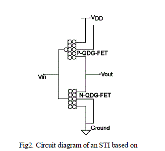
| The circuit diagram of QDGFET standard ternary inverter is shown in Fig 2. This circuit is the same as a conventional CMOS inverter, except that the transistors have been replaced by QDGFETs. In this circuit, when the input is 0, the P-QDGFET is in the ON state and the N-QDGFET is in the OFF state, which makes the output 2. When the input is 2, the P-QDGFET is OFF and the NQDGFET is ON, which make the output 0. When Vin is equal to 1, both transistors are in the intermediate mode, thus making both of them behave like a resistor. In this situation, the circuit behaves like a voltage divider which produces an intermediate logic output assuming both transistors have equivalent βs. This intermediate logic output depends on different parameters of both QDGFETs and their size ratios. In other words, changing the size ratio will produce different complement functions. |
 |
| The circuit diagram for the NTI and the PTI is same as in Fig. 4(a) where the QDGFETs are replaced by conventional pMOS and nMOS transistors with 22 nm feature size parameters. Based on the threshold voltage of pMOS and nMOS, the inverter can behave as a NTI or as a PTI. For NTI, the threshold voltage of the pMOS is −0.3 V and that of the nMOS is 0.11 V. When the input voltage is below 0.11 V, the nMOS is OFF and the output is 0.5 V. When the input voltage is above 0.11 V, nMOS is ON and the output is zero. For the PTI implementation, the threshold voltage of the nMOS and the pMOS should be 0.3 V and −0.2V, respectively. |
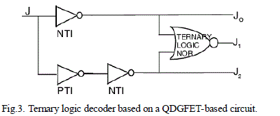
VI. TERNARY LOGIC DECODER |
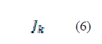
| Ternary decoder is a combinational circuit which decodes the input ternary signal. A ternary decoder is a one-input–three-output combinational logic circuit. The output of a ternary decoder can be represented as in (6) |
 |
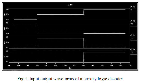
| Where k =0,1,2 which corresponds to higher level (2),middle level (1), and lower level (0). The design of the ternary decoder based on QDGFET is shown in Fig. 3 where we use two NTI gates, one PTI gate, and one ternary NOR gate. The output of the decoder is shown in |
 |
 |
 |
VII. 1 BIT COMPARATOR |
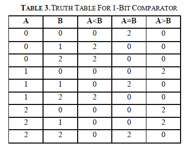
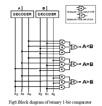
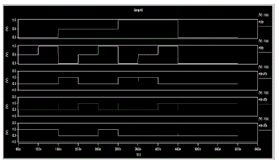
| A 1-bit comparator compares two ternary bits and produces three outputs based on the relation between the two input signals. There are three outputs: A >B, A=B, and A<B in the comparator circuits. Based on the relation between two inputs (A and B), corresponding output becomes high and others remain low. The block diagram and the input–output waveform of a ternary comparator is shown in Fig. 5 and 6, respectively. The truth table of the ternary comparator is shown in Table 2. |
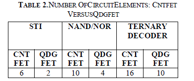
| Table 3 shows the required number of circuit elements to implement different logic circuits using CNTFET [14] and QDGFET. |
 |
 |
 |
| In this paper, we demonstrated the design of different ternary logic circuits based on QDGFETs. Less power dissipation was observed in the QDGFET-based ternary logic circuits than the other. The improved performance of the QDGFET-based ternary logic circuits was because of the fast resonant tunneling mechanism of the charge carriers from the inversion channel to the different layers of quantum dots in the gate region. We also did the comparative analysis of number of circuit elements required with QDGFET and CNTFET based circuit, which shows QDGFET based circuits requires less amount of circuit element compared with CNTFET. There will be uniform noise margin of the designed ternary logic circuits because of the less charge leakage between the quantum dots in the gate region of the QDGFET. This paper showed the improved performance of the ternary logic circuits based on the QDGFET because of the tunneling mechanism and the cladded dots in the gate region. The improved performance of the different QDGFET-based ternary logic circuits will make QDGFET a promising circuit element in MVL circuits in the future. |
References |
|