International Journal of Advanced Research in Electrical, Electronics and Instrumentation Engineering
ISSN ONLINE(2278-8875) PRINT (2320-3765)
ISSN ONLINE(2278-8875) PRINT (2320-3765)
Abhishek Pandey1, Divya Yadav2, Ritika Singh2, Vijay Nath (Member IEEE)3
|
| Related article at Pubmed, Scholar Google |
Visit for more related articles at International Journal of Advanced Research in Electrical, Electronics and Instrumentation Engineering
In this paper we are introducing novel Ultra Low Power CMOS temperature sensors for space applications. Nowadays for each & every application new standard circuits are required. This proposed CMOS temperature sensor is able to measure the temperature range from -150oC [-238 oF] to 260oC [500 oF]. This low power CMOS temperature sensor is able to work in harsh environment. It is gainsay to design wide range, linear response from -150oC to 260oC temperature sensor for different space applications such as environment cooling systems, oil in hydraulic and lubricating system and fluid in coolant and heating systems. This circuit is designed in concept of SoC and operates with a single rail power supply of 1V. This circuit power consumption is 0.752μW [-238 oF] and 46.7 μW [500oF] . The sensitivity of this circuit is about 0.18 μW/ oC. This paper based on Proportional to Absolute Temperature (PTAT) and Negative Temperature Coefficient (NTC). This circuit is designed & simulated using Cadence Analog & Digital system design tools UMC 90nm technology.
Keywords |
| CMOS: Complementary Metal Oxide Semiconductor; VLSI: Very Large Scale Integration Circuit; SOI: System on Insulator; SoC: Silicon on Chip. |
I. INTRODUCTION |
| Temperature is one of the most important fundamental physical quantities and is almost common in our daily life and which is independent of the amount of material i.e. temperature is having intensive property. As we know hundreds or thousands of devices are formed on thin silicon wafers. Before the wafer is scribed and cut into individual chips, they are usually laser trimmed. Process compensated CMOS temperature sensor [1] has designed for microprocessor application. The beauty of this circuit is no need of any BJT component. This CMOS temperature sensor is able to sense range -40oC to 85oC. The ultra low power CMOS cell temperature sensor [2] designed with PTAT (Proportional to Absolute Temperature) with NTC (Negative temperature Coefficient). This temperature sensor able to sense ranges 32oC to 127oC. |
| 0.6-2.0V CMOS temperature sensor [3] defined only bulk driven technology. This temperature sensor is designed to sense from 0 oC to 120 oC using UMC 0.13um technology. A single chip PTAT sensor [4] designed using CMOS technology. This temperature sensor having wider temperature range with excellent linearity. Its range is -100 oC to 200 oC and sensitivity is about 0.05mV/ oC. The chip is designed with a single voltage source 1.6V. It can be used in various applications. |
| Temperature is a physical quantity that is a measure of hotness and coldness on a numerical scale [5]. In a body in its own internal thermal equilibrium, the temperature is spatially uniform. Temperature is important in all fields of natural science. Temperature sensors are not only useful for space applications, but it has many more use in different areas such as physics, chemistry, geology, and biology etc. |
| As we know ICs designed chips from BJT are good in some operational conditions but there are problems of power dissipation and package density. Due to requirement of simplicity, reduced parasitic/latch-up and high package density we move in the direction on new technology CMOS SOI [6]. In CMOS circuit NMOS transistor are used as the best driver and PMOS as a load. Decreasing feature size and increasing package density cause self-heating of chips to become an important factor. Since by decreasing the gate length the latch-up/parasitic effect increases. Hence to reduce the latch-up/parasitic effect we intend to utilize CMOS SOI technology for the same purpose. This mentioned paper work aims at developing a low power micro system (MST) for continuous temperature monitoring with a longer life power harsh environmental condition. |
| In early days the diode and transistor their base-emitter voltage VBE related to temperature. The best performance of BJT (Bipolar Junction Transistor) is -50oC to 150oC for good linearity. Over 200oC the BJT junction is destroyed [7]. We are approaching CMOS PTAT (Proportional to Absolute Temperature) temperature sensor. In CMOS the threshold voltage and mobility are two main factors which are temperature dependent parameter. In the MOSFET the best thing is that we can scaling the parameter i.e. we can change doping, threshold voltage, mobility etc. As we know that in modern VLSI technology if we changes in channel length of transistor, then doping concentration, mobility, threshold voltage is also changes. If the threshold voltage or mobility is varies then temperature is also varies. A 405nW CMOS Temperature sensor is based on linear MOS operation [8]. This CMOS temperature sensor is suitable for ultra low power application with a MOS transistor operation in linear region, a linear relationship between delay and temperature can be obtained. |
| SOI CMOS technology is feasible for extreme temperature applications up to 225 oC [9]. This SOI CMOS temperature sensor is developed for radiation environments in aerospace applications. We proposed an ultra low power CMOS temperature sensor with excellent linearity. This CMOS temperature sensor expresses best linearity between -150oC [-238 oF] to 260oC [500 oF]. These circuits are many more feasible in space applications such as environment cooling systems, oil in hydraulic and lubricating system and fluid in coolant and heating systems. These circuits are designed on the concept of PTAT (Proportional to Absolute Temperature) with NTC (Negative temperature Coefficient). It is designed and simulated using Cadence analog and digital system design tools UMC 90nm technology. It is operational on very low single power supply 1V and its power consumption is 0.755μW [-238 oF] and 46.7 μW [500oF]. |
II. METHODOLOGY |
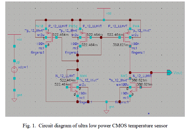
| Simple current mirror based circuit is shown in Fig.1. We know that when we connect the gate to the drain of MOSFET then it operates in saturation region [10]-[12]. Connecting the gate to the drain means that the DS V control D I and therefore the channel transconductance become a channel conductance. When NMOS transistor comes in saturation region then |
 |
 |
| From equation (13) it is clear that d r is inversely proportional to aspect ratio (w/l). Hence if we are increasing the value of aspect ration the value of resistance will be decreases. |
III. SIMULATION RESULT & DISCUSSION |
 |
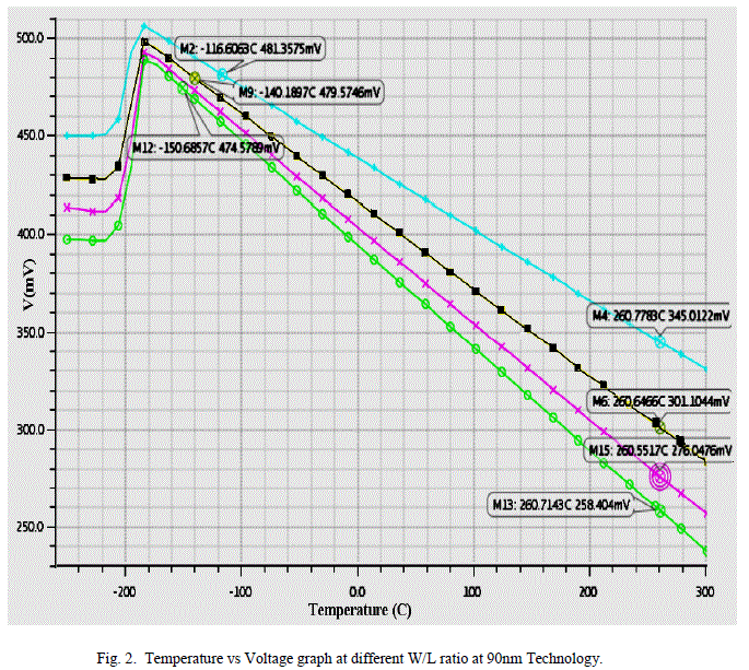
| A. At different w/l ratio |
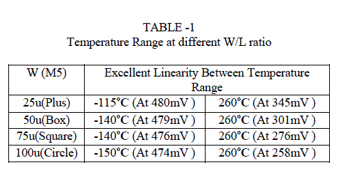
| In the Fig (1) transistor M4 and M5 work as load. We plotted the graph between Voltage and Temperature on different aspect ratio of M5 is shown in Fig (2). In simulation we increase the value of aspect ratio range 25u to 100u with constant increment of 25u. We achieved wider excellent linearity between the ranges -150oC to 260oC at the aspect 100u and the voltage difference between this two temperature ranges is also good. Aspect Ratio of all transistor are given below S1=S2=S3=2u/90n. S4=2u/90n, S5=Variable; and Power Supply Voltage VDD=1V. The temperature range at different aspect ratios is shown in table1. |
 |
 |
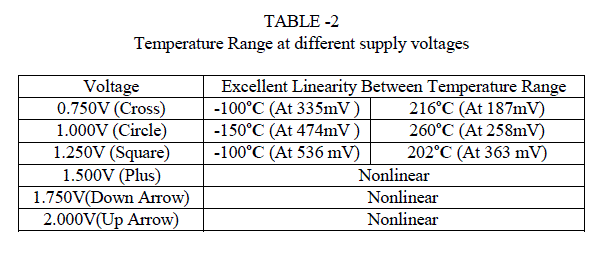
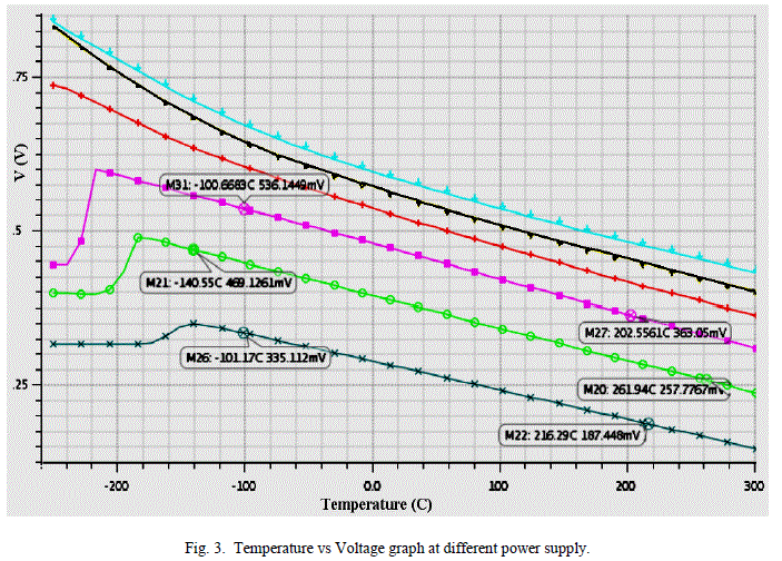
| B. At different power supply(VDD) |
| Fig.3 shows the range of temperature sensor at different power supply (VDD). Hence we are changing the voltage from 0.750V to 2.000 V with increment of 0.250V. We achieved better result at 1V fixed aspect ratio of all transistors. S1=S2=S3=2u/90n, S4= 2u/90n, S5=100u/90n. Temperature range at different supply voltage is shown in table-2. |
 |
 |
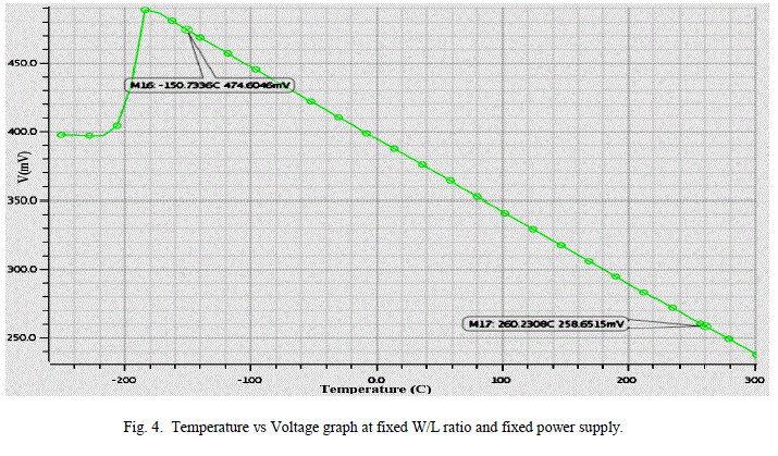
| C. At fixed w/l ratio and fixed powers supply |
| Fig.4 shows the fixed supply 1V and fixed aspect ratio of all Transistors. S1=S2=S3=2u/90nm, S4= 2u/90nm, S5=100u/90n. |
 |
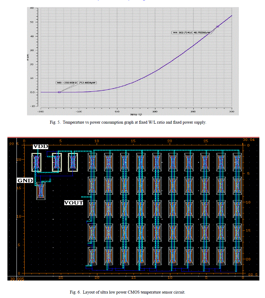 |
| Temperature vs power consumption graph at fixed W/L ratio and fixed power supply is shown in Fig.5. The layout of ultra low power CMOS temperature sensor is shown in Fig.6. Its layout area is 30mX 20.5m. |
IV. CONCLUSION |
| A ultra low power CMOS temperature sensor is designed with excellent linear range of -150 oC to 260 oC. The layout area of this circuit is 30ïÃÂÃÂmX 20.5ïÃÂÃÂm. The Circuit designed for fabrication in UMC Belgium with Cadence analog and digital system design tools with UMC 90nm technology. It is operational on very low single power supply 1V and its power consumption is 0.755μW [-238 oF] and 46.7 μW [500oF]. The sensitivity of this circuit is about 0.18 μW/ oC. |
ACKNOWLEDGMENT |
| We are thankful to Department of Science and Technology, New Delhi and Defense Research Development Laboratory Hyderabad India for funding this project. We are also thankful to our Vice-Chancellor, Dr. P.K. Barhai and our Head of Department of ECE, Dr. S.K.Ghorai for his constant inspiration and encouragement. |
References |
|