International Journal of Advanced Research in Electrical, Electronics and Instrumentation Engineering
ISSN ONLINE(2278-8875) PRINT (2320-3765)
ISSN ONLINE(2278-8875) PRINT (2320-3765)
| Siji Das1, Mrs.Jisha Kuruvilla2, Dr. Babu Paul3 |
| Related article at Pubmed, Scholar Google |
Visit for more related articles at International Journal of Advanced Research in Electrical, Electronics and Instrumentation Engineering
This thesis aims at end to end design of a push-pull dc-dc converter with analog PWM controller. The pushpull converter circuitry consist of a power transfer stage with an appropriate switching device. Rectifier and filter circuits are used for filtering and smoothening of the output dc voltage. The switch duty ratio is controlled by means of a PWM controller chip. To improve the system stability and to obtain desired bandwidth compensation circuit is incorporated. EMI filters (both common mode and differential mode) are used to avoid unwanted signals in the circuit. The complete circuit is modelled and simulated to check the adequacy of the design. Circuit modelling and simulation is carried out by I-CAP4 simulation package.
Keywords |
| dc-dc converter, PWM controller, compensators, EMI filters, I-CAP4 |
INTRODUCTION |
| A dc-dc converter [1] is an electrical device that converts an unregulated dc input voltage into a well regulated output, typically within awell-defined tolerance level. The converter circuitry may be of isolated or non-isolated depending on the input and the output requirements. The circuit will usually consist of a power transfer stage with appropriate switching devices along with necessary input and output filters, feedback circuit, PWM controllers and compensators[2]. An increase of the system frequency [3] causes a considerable reduction in both size and cost of the associated components |
| The thesis work aims at developing a complete converter circuitry that operates at high frequency.The basic block diagram of the proposed dc-dc converter is shown in fig.1. |
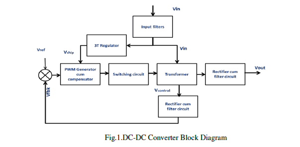 |
| The converter circuitry was implemented using a push pull converter topology. This topology provides better input output isolation for the circuit at reduced cost. Also this arrangement can meet the requirement of multiple outputs whenever required. Buck & Boost converters do not have isolation and power limit is <100W. Fly back converter & forward converter recommended operating power is <150W and switching transformer core size to be larger by a factor of 2 in comparison with push-pull. Half bridge recommended power is 100-500W but the peak current through the switch at the same power is double that of push-pull. Also the no. of parts are higher compared to push-pull. Full bridge is meant for very high power and no. of parts are high. Hence push-pull topology is selected . |
| The main advantages of the proposed circuit are that the input EMI filters[4] incorporated into the circuit provide it better isolation from common and differential mode noises from outside interferences, compensation circuitry incorporated to the PWM generator improve the system stability by avoiding feedback loop oscillations. These advantages make the circuit useful for a wide range of applications including space shuttles, solar panels etc. |
| The developed circuitry has been simulated by using ICAP-4[5] circuit simulation package to check the accuracy of the design and the results have been studied. The simulation results are validated by conducting experimental results. |
II. DESCRIPTION OF DC-DC CONVERTER SWITCHING SYSTEM |
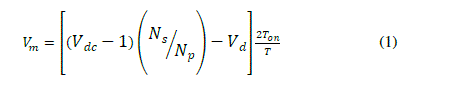
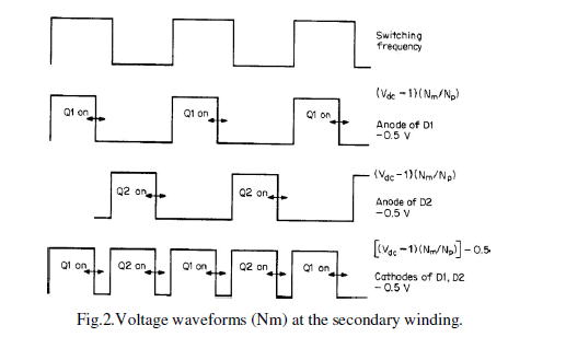
The switching circuit for the dc-dc converter consist mainly of a fast acting Push-Pull switching transformer that will change the supply voltage level to a different output voltage level as per the requirement. It consists of a transformer T1 with multiple secondary’s. Each secondary delivers a pair of 180âÃâæ out-of-phase square-wave power pulses whose amplitude is fixed by the input voltage and the number of primary and secondary turns. The pulse widths for all secondaries are identical, as determined by the control circuit and the negative-feedback loop around the master output. Transistor base drives at turn “on” are sufficient to bring theswitched end of each half primary down to Vce(sat) , typically about1 V, over the full specified current range. Hence as each transistorturns “on,” it applies a square-voltage pulse to its half primary ofmagnitude (vdc-1) On the secondary side of the transformer, there will be flat-topped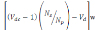 ith a duration To , where Vdis an output rectifier forward drop, taken as 1 V for a conventional fast-recovery diode, and 0.5 V for a Schottky diode. The output pulses at the rectifier cathodes have a duty cycle of 2Ton/T because there are two pulses per period. ith a duration To , where Vdis an output rectifier forward drop, taken as 1 V for a conventional fast-recovery diode, and 0.5 V for a Schottky diode. The output pulses at the rectifier cathodes have a duty cycle of 2Ton/T because there are two pulses per period. |
| Thus the waveforms at the inputs to the LC filters are very much like that at the input to the buck regulator LC filterof Figure 1, which has a flat-topped amplitude and adjustable width. The LC filters provide a DC output that is the average of the square wave voltage at the input of the filter. The analysis of the inductor and capacitor functions proceeds exactly as for the buck regulator, and the method of calculating their magnitudes is exactly the same as follows. The DC or average voltage at the Vmoutput in Figure 2 will be |
 |
| The waveforms at the Vmoutput rectifiers are shown in Figure 2. |
 |
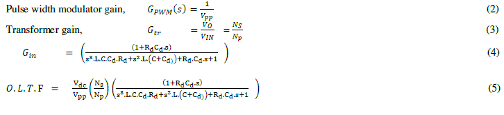
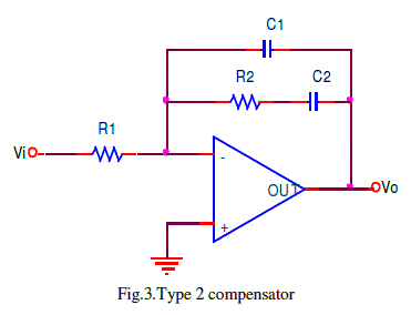
| The PWM generators is responsible for controlling the switch turn on and turn off so as to maintain the output within the prescribed tolerance level.Usually the circuit are with negative feedback loop and thus provides negative feedback and a stable output voltage at low frequencies. Within the loop, however, there are low-level noise voltages and voltage transients possible, which have a wide spectrum of sinusoidal Fourier components. If one of these Fourier components has a loop gain of 1 and a phase shift of a further 180âÃâæ (the first 180 being provided by the negative feedback connection), the total phase shift will be 360âÃâæ. Then the feedback signal will be in phase with the original input, resulting in positive rather than negative feedback, which will result in oscillation.The compensation circuitry incorporated into the system is used to avoid the feedback loop oscillations. The compensation circuit will increase the system stability margin and thus improves system stability and reduces the feedback loop oscillations. But eventually the system response timings will also increase. |
| The compensator circuitry was designed by analysing the system open loop response. The system transfer function is obtained as below: |
 |
 |
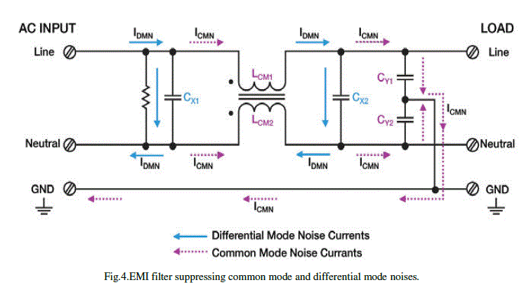
IV. INPUT FILTERS |
| DC-DC converters can generate and/or be affected byEMI. Sources are everywhere and include ac motors, fluorescent bulbs/ballasts, light dimmers, microwaveovens, microprocessors, computers, and switch-mode power supplies.Within switch-mode power supplies, a high dc voltage is chopped orswitched at a high frequency that can range from 50 kHz to 1 MHz. This high-speed switching process isintrinsic to switch-mode power supplies and provides its improved efficiency and reduced size when compared to linear power supplies.However, as a side effect, this switching generates unwanted EMI. Infact, most conducted EMI within switch-mode power supplies originates from the main switching MOSFETs, transistors, and output rectifiers |
| Conducted EMI is divided into two main types: Common-mode noise (CMN) and differential-mode noise (DMN). CMN, a.k.a. asymmetrical noise or line-to-ground noise, exists on both sides of the ac input (line and neutral), in-phase with itself relative to ground. The CMN current flows in the same direction on both power conductors and returns via the ground conductor. CMN can be suppressed by the use of inductors within an EMI filter that are placed in series with each power line and by Y-capacitors that are connected from both power line conductors to ground. |
| CMN is suppressed by using dual-wound toroid type inductors (LCM1 and LCM2).These inductors are wound on a single core in such a way that they present a high impedance to the in-phase common-mode noise on each ac conductor. In addition, the Y-capacitors (CY1 and CY2) shunt or bypass the high-frequency common mode noise to ground. |
| DMN on each ac conductor is suppressed by the two X-capacitors (CX1and CX2), which tend to neutralize the outof- phase high-frequency DMN that exists between the ac power line and neutral conductors. The input resistor discharges these capacitors when the power is turned off. |
 |
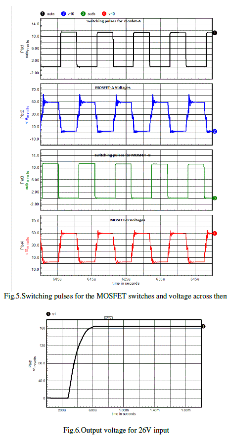
V. SIMULATION RESULTS |
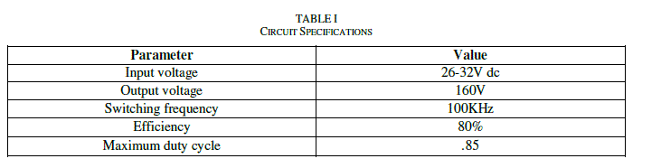
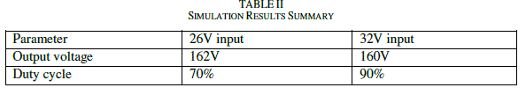
| The designed circuit was simulated using I-CAP4 circuit simulation package and the results are studied.The design circuit specifications are given in table. |
 |
 |
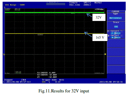
| B.Results for 32V input |
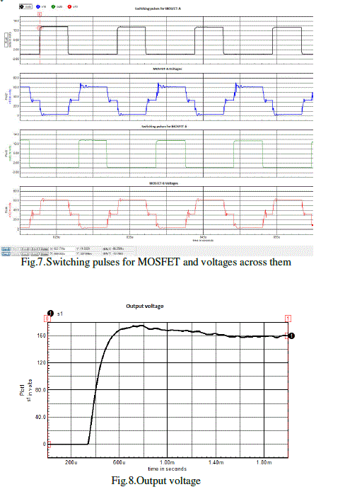 |
| The results obtained after simulation is summarised in the table.2. |
 |
VI. EXPERIMENTAL RESULTS |
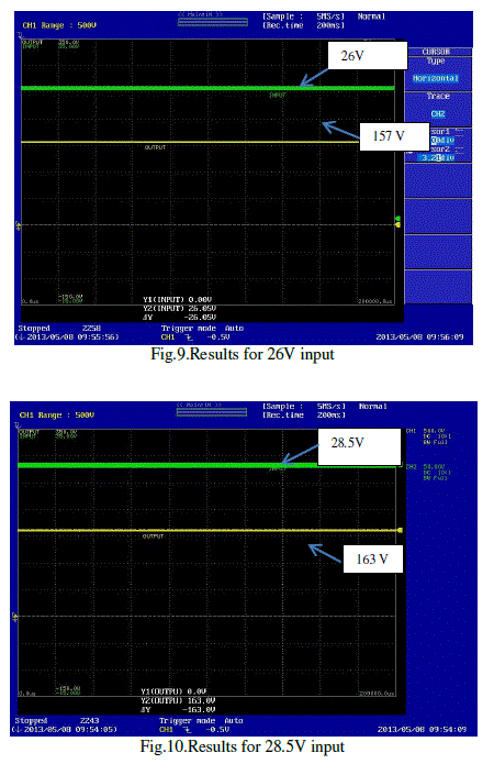
| The circuit was validated by conducting experimental setup. The circuit was set up on a prototype chip and the input voltage is varied within prescribed limits. The result obtained shows a close match with the simulation results. |
 |
 |
VII. CONCLUSION |
| In this paper the complete design of a high frequency DC-DC converter has been developed using push pull topology. EMI filters incorporated into the system make it isolated from the common mode and differential mode noises. Also addition of compensation circuitry improves the system stability. The simulation results have shown that the system the system can well regulate its output within a prescribed tolerance under the specified input supply variations. The results are then validated by conducting experimental setup. |
References |
|