Research & Reviews: Journal of Material Sciences
ISSN:2321-6212
ISSN:2321-6212
Dhiflaoui H*, Khlifi K and Cheikh larbi AB
National High School of Engineers of Tunisia, University of Tunis, 5 Taha Hussein Street, 1008 Tunis, Tunisia
Received Date: 20/05/2016; Accepted Date: 30/06/2016; Published Date: 08/07/2016
DOI: 10.4172/2321-6212.1000148
Visit for more related articles at Research & Reviews: Journal of Material Sciences
In the current study, TiO2 coatings on stainless steel substrates were prepared by Electrophoretic Deposition (EPD) of colloidal dispersions of TiO2 nanoparticles in ethanol. The effects of deposition parameters on surface morphology, phase composition and mechanical properties were investigated. The surface morphology of the EPD layers was observed using Atomic Force Microscopy (AFM). The composition of the EPD layer was determined from the peak intensity using an X-ray Diffractometer (XRD) and mechanical properties of films were investigated by nanoindentation techniques. Characterization of the obtained films by atomic force microscope showed a relatively uniform microstructure. The coatings mainly consisted of anatase and rutile; anatase is the predominant phase with an average percentage of 71%. As a result of nanoindentation experiments, load–displacement curves were obtained and two mechanical characteristics of the substrate and investigated films – indentation hard-ness (HIT) and indentation modulus (EIT) – were calculated using Oliver & Pharr’s approximation methods. Mechanical properties show an improvement with the applied voltage. The results illustrate that Young's modulus and hardness of TiO2 thin films are increased with increasing voltage.
Nanoparticles, Ceramic materials, Parameters, Atomic force microscopy.
The Electrophoretic Deposition (EPD) technique is a widely used technique for novel applications in the processing of advanced ceramic materials and coatings. It has recently become the interest of both academic and industry fields because of its advantages such as: applicability to large areas, simplicity in setup, easy coating into conductive substrates, good control of coating thickness, short formation time and low cost equipment [1-4].
Electrophoretic Deposition (EPD) is an electrochemical process used to deposit coatings on a substrate electrode from colloidal particles suspended in a liquid medium; it is based on the movement of charged particles in an electric field. The particles move toward the working electrode due to the applied cell voltage and their accumulation on this electrode leads to the formation of a homogeneous layer.
Titanium oxide coatings are very important materials with numerous commercial applications such as self-cleaning glazing [5], water purification [6], sensors [7], photo-catalyst and photovoltaics [8,9], corrosion protective coatings [10] and coatings for biomedical applications [11-14].
EPD continues to attract attention for the deposition of uniform coatings on [15,16], and for the deposition of films from nanoparticles and carbon nanotubes [17,18].
In order to improve the wear and corrosion resistance of materials, some researches focused on the development of thin films [19-22].
Until today, finding a way to improve the wear resistance and surface hardness was the main subject of many research activities. Developing hard coatings, such as TiO2, appears to be an effective way to improve the mechanical properties of the surface. Only a few papers investigated the mechanical properties deposited by Electrophoretic Deposition, which is the subject of this work. Indeed, researchers have adopted the nanoindentation method to study the mechanical properties of thin films, because the nanoindenter generally has an excellent force of resolution and control better than 1.0 mN and an excellent displacement resolution better than 0.1 nm [23,24].
Niazi et al. [25] have investigated the TiO2-Al2O3 coatings deposited under different voltages. It shows that at higher voltages the differences between values of microhardness are more obvious due to the incorporation of more alumina nanoparticles at higher voltages, microharness increases from 300 Hv with voltage of 250 V to 900 Hv with voltage of 450 V. The hardness of the TiO2–ZrO2 nanostructured composite coatings by EPD-Enhanced MAO (EEMAO) technique shows that hardness increases with processing time as well as the zirconia concentration [26].
This paper reports the successful fabrication and characterization of TiO2 thin films. It investigates the morphology, the micro-structural parameters like crystallite size, mechanical properties and the relationships between all of these parameters of TiO2 coating.
Substrate Pre-treatment
This study focuses on stainless steel electrodes discs type 316L with a diameter of 15 mm and a thickness of 3 mm. Samples were mechanically polished from 120 to 1000 grit Silicon Carbide (SiC) papers followed by a diamond pastes to get mirror finish (Table 1). The electrodes were washed thoroughly with running distilled water, rinsed and ultrasonically degreased with acetone and dried for 10 min [27].
| Element | Cr | Ni | Mo | Si | Mn | P | S | C | Fe |
|---|---|---|---|---|---|---|---|---|---|
| Wt.% | 17-21 | 9-13 | 2-3 | 1.5 | 1.5 | 1.5 | 0.04 | 0.03 | Bal |
Table 1: The nominal composition of 316L stainless steel.
Preparation of TiO2 Suspensions
Thin TiO2 films are deposited on 316L stainless steel substrates using the EPD technique TiO2 powder from Aldrich is used (Sigma-Aldrich Corporation, St. Louis, MO, USA), where 99.7% of the particles have dimensions less than 25 nm. The electrolyte solution is composed of a mixture of 0.06 g of TiO2 nanopowder with 60 ml of absolute ethanol where ≥99.8%. An aluminum plate with a dimension of 20 X 15 mm2 was used as a counter electrode (anode). Each electrode was submerged into the prepared media with a 1 cm distance. The plating bath compositions and deposition parameters are illustrated in Table 2. The suspensions were magnetically stirred for 5 min followed by 15 min ultra-sonification, subsequently followed by 5 min of stirring.
| Item | Parameters |
|---|---|
| Temperature | 25°C |
| Pulse frequency | 1 kHz |
| Duty cycle (pulse on time) | 50% |
Table 2: Plating bath compositions and deposition Parameters.
The deposition yield (deposited mass/covered area) was evaluated for AC-EPD coatings in dependence of varying deposition time and voltage.
Particle deposition and heating
Each electrode was submerged into the prepared media at 25°C. For AC-EPD tests, a generator (HP 3314A) was used to generate the asymmetric AC signal. A Piezo Driver/Power amplifier (PZD 700A) with a maximum voltage of 700 V in DC or peak AC was used to amplify the signal. The signal was monitored with a digital oscilloscope (Tektronix). Different voltages from 20 to 40 V and times from 3 to 5 min were considered to obtain electrophoretic coatings.
The deposited substrate was heated to 650°C for 4.5 h with a heating rate of 2.5°C/min in a furnace to evaporate any organic or volatile components. A desirable temperature due to the possible transformation of the anatase phase in the TiO2 particles will be converted to the rutile phase [28]. This would cause substrate contamination [29] and grain growth [30]; that causes the change in mechanical property of deposit ceramic layer.
The surface morphology of TiO2 films production was analyzed by atomic force microscopy (AFM, Model Nanoscope III). Tapping mode images were obtained in air using Silicon Nitride tips (TESP, Nanosensors) with a maximum radius of curvature of 10 nm and spring constant k=42 N/m.
Film surface parameters such as root mean square roughness Sq, average roughness Sa and the peak-to-valley height St which were analyzed from AFM images. The phase structure of the synthesized coatings were studied by X-ray diffraction technique where a Rigaku Multiflex instrument equipped with a Cu-Kα X-ray source (λ=1.54178Å) was used.
Mechanical properties of TiO2 films were investigated by nanoindentation experiments, using Nano Indenter NHT2 (CSM instruments, Suisse). The nanoindenter is equipped with a Berkovich diamond pyramid with a nominal angle of 65.3° and a nominal radius curvature of 20 nm radius at the tip of the indenter. The minimum allowed load is 0.1 mN, and the maximum load is 500 mN. Displacement recording resolution is 0.01 nm and the load recording resolution is 50 nN. The device is equipped with an optical microscope with 3 objectives with magnifications of 200×, 800× and 4000×. Hardness and modulus are determined using stiffness calculated from the slope of the load–displacement curve during each unloading cycle. As a result of nanoindentation experiments, load–displacement curves were obtained and two mechanical characteristics of substrate and investigated films – indentation hardness (HIT) and indentation modulus (EIT) were calculated using Oliver & Pharr’s approximation method [31].
Five indentations were made at a constant maximum load of 80 mN and the mechanical properties values were averaged to obtain the mean value. It has been demonstrated that an indentation depth of less than 10% of the film thickness helps to avoid substrate contributions to film’s mechanical properties [32].
Surface Morphology of TiO2 Coatings
The EPD coatings after the thermal post treatment at 650°C in air were observed with an optical microscope (Figure 1).

Figure 1: Optical microscope images of EPD coatings at different voltages and deposition times.
To prepare the most appropriate nano-TiO2 coating, the effects of two experimental deposition parameters were explored. First, the variation of the potential was studied at 20, 30 and 40 V.
Nevertheless, as shown in Figure 1, there are some cracks with approximate width of 0.5 μm within the layer. However, some closer observations of these samples reveal that the coatings deposited at 30 and 40 V are highly cracked, whereas, the coatings deposited at 20 V are confirmed to be the most homogeneous. The approximate width of the cracks is about 2.5 μm which is obviously larger than that of the coatings deposited at 20 V. These observations indicate that the two potentials 30 and 40 V do not lead to an adequate agglomeration at the surface of the substrate, resulting in the formation of several cracks [33].
Thus, it is obvious that the potential of 20 V is most suitable. Next, the selected voltage (20 V) was used to test the effect of various deposition times: 3, 4 and 5 min. For a 3 min time deposition, it appears to be too low to yield a coating that properly covers the surface. After 5 min, a coating with a maximum homogeneous surface was obtained, whereas, the samples present some cracks and some uncovered areas. This could be attributed to the higher thickness of the film in longer EPD times and it is more probable to crack during the solvent evaporation. After 4 min, a coating with a maximum homogeneous surface was obtained.
According to these results, the best electrophoretic deposition conditions were established to be at 20 V for 4 min that defines then the best nano-TiO2 coating for microstructural and morphological studies.
Optical microscope images of a cross section of the TiO2 coating are given in Figure 2. It shows that the interface between the TiO2 film and the stainless steel substrate is very good. The coating thickness is in the range of 25 μm.

Figure 2: Cross-section images.
Electrophoretic deposition yield curves for coatings obtained by AC-EPD at different conditions are shown in Figures 3 and 4.

Figure 3: Deposition yield for TiO2 coatings showing the expected increased deposition with time at fixed voltage.

Figure 4:Thickness for TiO2 coatings showing the expected increased thickness with time at fixed voltage.
Figure 3 shows the deposition yield increasing with increasing time depositions and voltage at a fixed frequency of 1000 Hz. The deposition yield increases linearly with time at each applied voltage. Generally, keeping constant with the other parameters, the yield of the deposit increases with increasing applied voltage. It is due to the higher particle mobility caused by the greater potential difference between the electrodes [34].
A higher applied field may cause turbulence in the suspension and the coating that may be disturbed by surrounding media motions. The results support the Hamaker essentially linear model EPD described by the following equation.
 (1)
(1)
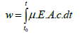
Where is the deposit yield (in g), E is the electric field (in V/m), is the electrophoretic mobility (in m2/V/s), A is the surface area of the electrode (in m2), c is the particle mass concentration in the suspension (in g/L) and t is the deposition time (in s).
Figure 4 shows the increasing trend of the thickness with increasing time depositions at different applied voltage and at a fixed frequency of 1000 Hz.
Figure 5 shows X-ray diffractograms of TiO2 coatings at 5 min (Figure 5a) and 4 min (Figure 5b) with different voltages. The diffraction pattern of TiO2 coatings shows peaks of anatase phase located at 2θ=25.35°, 37.90°, 48.10°, 55.13°, 68.97° corresponding to the (101), (004), (200), (211) and (116) crystal faces, respectively (JCPDS no 01-089-4921) . The corresponding X-ray diffraction (XRD) pattern in Figure 5b shows peaks at 27.50°, 36.15°, 54.19°, 62.78°, corresponding to the (110), (101), (211) and (002), attributable to the TiO2 rutile structure (JCPDS no 01-089-4920).

Figure 5: XRD patterns of TiO2 at different time depositions a) 5 min, b) 4 min.
Results show that intensity of the phase’s characteristic peaks increased with voltage. Furthermore, the intensity of the XRD lines from the rutile phase’s changes at varying applied voltages. The phase transformation of anatase to rutile depends on the electric current in the electrochemical cell [35]. The reason for the transformation of anatase to rutile is the changes in electric current.
The grain size was calculated by using Debye-Scherer’s formula from the full-width at half maximum (FWHM) of the (101) reflection [36-38]:
 (2)
(2)
Where D is the crystallite size or grain size,λ is the wavelength of X-ray, B is the full width at half maximum of diffraction peak and θ is the diffraction angle.
The average grain size is about 23 nm. It presents an increasing trend with increasing voltage. Grain size increases from 23.15 nm to 24.67 nm and from 20 V to 40 V.
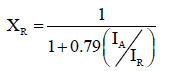
Following the method reported by Shah [39], the mass fraction of rutile (XR) in TiO2 films prepared by EPD, were calculated based on the relationship that exists between the integrated intensities of anatase (101), IA, and rutile (110), IR, peaks in Spurr's equation.
 (3)
(3)
The results of XRD data analysis are shown in Table 3 where it can be seen that, as expected, the fraction of rutile XR and anatase XA, does not change in an important fashion either by EPD time or voltage.
| Voltage | |||
|---|---|---|---|
| 20 V | 30 V | 40 V | |
| XA (%) | 71.9 | 71.8 | 71.7 |
| XR (%) | 28.1 | 28.2 | 28.3 |
Table 3: Effects of voltage on the phase structure.
Nano-Mechanical Properties
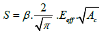
Nanoindentation tests were performed to measure hardness and modulus of film’s elasticity. The measurements of the hardness and Young’s modulus are mainly unloading curve based according to Oliver-Pharr’s method [31]. The unloading curve plays a key role in the analysis of the hardness and the elastic modulus (Figure 6). During unloading, the penetration depth decreases with the applied load, and when the indenter is completely removed, the residual depth hf is obtained. S is the contact stiffness (dP/dh) at the maximum load.

Figure 6: Typical indentation loading–unloading curve.
 (4)
(4)
Where AC stands for the projected contact area of the indenter tip.
Young's modulus of coating E is calculated from Hertzian equation:
 (5)
(5)
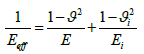
Where  and are the Poisson's ratios for the indenter and coating, respectively; Ei and E are Young's modulus for indenter and coating. In this study, it is assumed that =0.07 and Ei=1140 GPa for the diamond indenter.
Figures 7 and 8 show that the hardness and elastic modulus of the films as a function of voltage and deposition time. These results show that with increasing voltage, hardness and modulus increase. Modulus of elasticity and hardness increase from 16.77 GPa to 31.08 GPa and from 88.25 MPa to 254.31 MPa, with increasing voltage from 20 to 40 V.

Figure 7: Hardness of the films as a function of voltage and time depositions.

Figure 8: Elastic modulus of the films as a function of voltage and time depositions.
These effects can be explained by the elevation of deposit amount due to the kinetic deposition. Indeed, higher electric field promotes more TiO2 deposit on substrate which reduces void fractions and increases film compactness. On the other hand, the increase of voltage increases the fraction of rutile phase (Table 3); rutile phase is more suitable in providing enhanced mechanical properties [40]. Hardness and modulus increases (from 88.25 MPa to 254.44 MPa and from 16.77 GPa to 29.09 GPa, respectively) when the deposition time is increased for a fixed voltage. It can be explained by the increasing of film densification [41].
AFM analysis
The surface morphology of TiO2 films was analyzed by atomic force microscopy (AFM, model Nanoscope). Micrographs were obtained in tapping mode under ambient conditions, using high resonance frequency SiN cantilevers, with a pyramidal tip of 10 nm radius and a force constant of 0.032 N/m.
Figure 9 shows typical three-dimensional representations (0.1 μm x 0.1 μm surface plots) of TiO2 coated samples. AFM reveals a rough surface texture consisting of particles fused together at the inter-particle contacts and deep valleys. It can be observed from Figures 1 and 9 that voltage and time depositions have a direct impact on the grain size and morphology of the deposited films. The Rms (Rms: the standard deviation of the Z values, Z being the total height range analyzed) values of the TiO2 films show that the surface roughness increases as a function of voltage and time depositions [42]. Rms increases from 39 to 50 nm for 20 and 40 V at a constant time deposition (3 min), and from 40 to 70 nm for 3 and 5 min at constant voltage (40 V) (Figure 10).

Figure 9: Three-dimensional AFM images: a) 20 V, 3 min b) 20 V, 4 min c) 20 V, 5 min d) 30 V, 3 min e) 30 V, 4 min f) 30 V, 5 min g) 40 V, 3 min h) 40 V, 4 min i) 40 V, 5 min.

Figure 10: Roughness as a function of voltage and time depositions.
Titanium oxide films were elaborated by electrophoretic deposition methods and characterized by means of AFM, XDR and nanoindentation techniques. It has been demonstrated that the films morphological, phases’ composition and mechanical properties are dependent on their synthesis and processing conditions. The major conclusions can be summarized as follows:
1. Microstructure shows that cracking in thin films of TiO2 has been increased with increased voltage and time depositions.
2. The coatings consist mainly of anatase and rutile phases. The XRD analysis shows that the fraction of rutile XR and anatase XA has been 28.2% and 71.8%, respectively.
3. Mechanical nanoindentation testing shows a significant increase in hardness and Young’s modulus with increase in deposition parameters. The hardness and Young’s modulus can be up to 387 MPa and 40 GPa, respectively.