International Journal of Advanced Research in Electrical, Electronics and Instrumentation Engineering
ISSN ONLINE(2278-8875) PRINT (2320-3765)
ISSN ONLINE(2278-8875) PRINT (2320-3765)
Mr. Abhishek Verma1, Dr. Anup Mishra2, Arpita Jha3 and Kritika Verma3
|
| Related article at Pubmed, Scholar Google |
Visit for more related articles at International Journal of Advanced Research in Electrical, Electronics and Instrumentation Engineering
Over the past three decades CMOS has emerged as the basis of design in nanotechnology. MOSFETS provide an easier way of fabrication due to their ease of manufacturing and lower power consumption than the BJTs. However the use of high k materials to follow Moore’s Law, has created certain problems in the working of these devices. In this review we have dealt with the mobility related issue, which has been a major cause of concern. The degradation of mobility due to Coulomb scattering, Phonon scattering and other methods have been focused upon. The remedies of mobility improvement have also been highlighted. This review entails about the basic details of mobility in these devices with SiO2 and also with other high k materials. There are certain mechanisms which wrongly measure the count of charge carriers and give an overestimation or underestimation of the mobility, causing serious concern. The errors in mobility calculation and the overestimation of carrier count is a part of this review.
Keywords |
| Coulomb scattering, Phonon scattering, Carrier trapping, mobility. |
INTRODUCTION |
| Over the past three decades, CMOS technology scaling has been a primary driver of the electronics industry and has provided a path towards both denser and faster integration. The transistors manufactured today are 20 times faster and occupy less than 1% of the area of those built 20 years ago. The number of devices per chip and the system performance has been improving exponentially over the last two decades according to Moore’s law. As the channel length is reduced, the performance improves, the power per switching event decreases, and the density improves. But the power density, total circuits per chip, and the total chip power consumption has been increasing. |
| The need for more performance and integration has accelerated the scaling trends in almost every device parameter, such as effective channel length, gate dielectric thickness, supply voltage, device leakage, etc. SiO2 has been used as a gate oxide material for decades. As the thickness scales below 2nm, leakage currents due to tunneling increase drastically, leading to high power consumption and reduced device reliability. Replacing the silicon dioxide gate dielectric with a high-K material allows increased gate capacitance without the associated leakage effects. Since it becomes necessary to replace the SiO2 with a physically thicker layer of oxides of higher dielectric constant (K), there are various oxides under consideration for this purpose such as HfO2, hafnium silicate, ZrO2 and various lanthanides and it was found that in many respects they have inferior electronic properties than SiO2, such as a tendency to crystallize and a high concentration of electronic defects. The objective of using high-k oxides in place of silicon dioxide is to create smaller and faster devices. The speed of the device follows source to drain current, which in turn depends on the carrier mobility. The effective mobility μeff is defined in terms of the measurement of drain current , in the linear region as: |
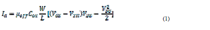 |
| where, |
| Cox , is capacitance of oxide, |
| W is width of oxide, |
| L is the channel length, |
| VGS is gate voltage, |
| VTH is threshold voltage, |
| VDS is drain voltage. |
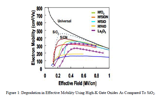
| One of the serious issues in high-k/metal gate stacks is degradation of effective mobility. CMOS devices with SiO2 gate oxide have mobility close to 300 cm/V-s for the electric field and doping concentration used. The mobility offered by high K oxides is below this value. It can be easily expected that effective mobility is reduced with high-k directly in contact of Si as shown in figure 1. The mobility is limited mainly by interface roughness over the range. |
 |
MOBILITY DEGRADATION |
| Mobility degradation is one of the crucial drawbacks of using high–K materials as a gate oxide as an alternative to SiO2 in Metal Oxide semiconductor field effect transistors (MOSFET). There are certain mechanisms of decline in mobility of the charge carriers. This entails to the internal mechanisms of the device which has to be studied carefully and can be observed only after careful scrutiny. There are certain remedies which can make up to the drawback of decrease in mobility, which are discussed at the end of this review. |
| The observations made by Takegi et al. [3] suggested that the mobility of electrons and holes depends only on the effective gate field and Si surface [5]. The individual components of mobility add according to Matthiessen’s rule, |
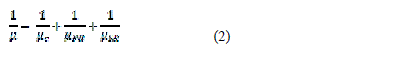 |
| where, |
 |
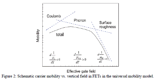
| The mobility is limited by different mechanisms at different fields, as each obeys a different power law with field. At low fields, mobility is limited by Columbic scattering(C) by trapped charges in the oxide, channels and gate electron interface; at moderate field it is limited by phonon scattering (PH), and at high fields by scattering by surface roughness (SR) as shown in figure 2. [4] The main focus is on Coulomb scattering due to interface traps and Phonon scattering due to soft optical phonons. |
 |
| A. Coulomb scattering |
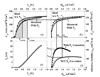
| The coulomb scattering due to interface trapped charge is the dominant mechanism of mobility degradation of highk gated MOSFETS at low fields. This is due to the fact that the energy distribution of the interface traps is found to be asymmetric as shown in figure 4. |
 |
| The interface trap density near the conduction band edge is higher than that near the valence edge as revealed by the larger sub-threshold swing of the n-MOSFET as compared to that of the p-MOSFET. Hence, the degradation of hole mobility in p-MOSFET is generally less severe than that for electron mobility in n-MOSFET as shown in fig. Coulomb scattering is mainly due to the electrostatic forces on the electrons when present in electric field. |
| B. Phonon scattering |
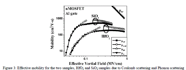
| In addition to Coulomb scattering caused by high densities of interface traps and oxide charge, the scattering due to soft optical phonons is a fascinating possibility that can’t be denied and the possibility is captured in figure. As shown in figure the mobility limited by phonon scattering in HfO2 gated MOSFETS is lower than SiO2 gate oxides. MOSFETS with several high-k oxides such as HfO2 has an additional source of phonon scattering. |
METHODS TO IMPROVE MOBILITY |
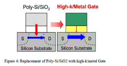
| The problem of mobility degradation can be overcome by substituting the poly-silicon gate electrode with metal gate as shown in figure 4. The conductivity of the poly-silicon layer is very low and because of this low conductivity, the charge accumulation is low, leading to a delay in channel formation and thus unwanted delays in circuits. The poly layer is doped with N-type or P-type impurity to make it behave like a perfect conductor and reduce the delay. Doped poly-silicon is a semiconductor, and thus will form a "depletion" region when voltage is applied. This "depletion" region acts very much like a thicker oxide, in that it reduces inversion charge (thus reducing inversion capacitance) with resulting degradation in drive current. |
 |
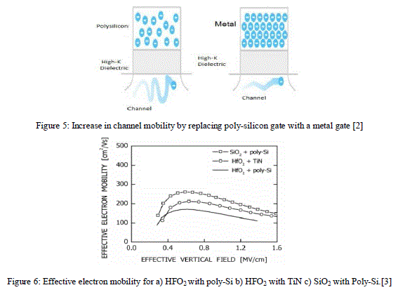
| The metal gate have free carrier density more than 1×10²⁰/cm3, which makes it possible to dynamically screen the longitudinal soft optical phonon modes arising from high-K dielectric materials. The metal gate electrodes help to screen the dipole coupling of remote phonon scattering. Thus are able to decrease phonon scattering and reduce the mobility degradation problem. The influence of dipole vibrations on the channel electrons can be reduced significantly by increasing the density of electrons in the gate electrode. Figure 5 shows how mobility is increased by replacing poly- Si with metal gate. Thus high-K oxides with metal gate have higher mobility than with poly-Si gate. In figure 6 it can be seen that HfO2 with metal gate have improved mobility |
 |
MOBILITY MEASUREMENT AND CORRECTIONS |
| The effective mobility, μeff, can be obtained by measuring the drain current in the linear region. |
 |
| Where Cox, is the oxide capacitance per unit area. This C–V stretch out effect would result in an over estimated inversion charge [3]. In this thesis, we propose a simple method to correct this error without having to measure the interface-trap density. The effects of channel resistance in weak inversion, gate leakage current, and contact resistance on the mobility extraction are also presented in this thesis, as they are distinctly different from the effects of interface traps. |
ACCURATE MEASUREMENT OF MOSFET WITH ULTRA-THIN HIGH-K DIELECTRICS |
 |
 |
 |
 |
 |
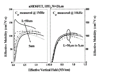 |
| Figure 8: Mobility values of HfO2 -gated n-MOSFET with various channel lengths extracted from split C–V measured at (a) 1 MHz and (b) 10 KHz. |
| As one can see, there is significant channel length dependence of the extracted mobility, especially in the weak inversion region. Thus, the effects of interface traps and channel resistance determine the lower and higher limits of the measurement frequency respectively. |
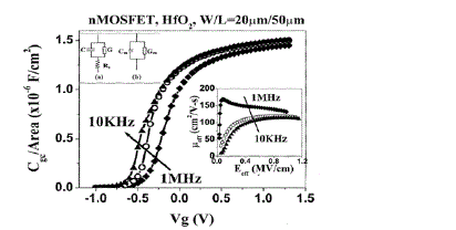 |
| Figure 9: Gate-to-channel capacitances of HfO2 -gated n-MOSFET with L =50μm measured at three different frequencies. The upper inset shows (a) the equivalent circuit model of the MIS capacitor and (b) the model for parallel capacitance measurement. The lower inset shows the apparent mobility values of this device as extracted from this set of split-C–V curves. |
| C. Contact Resistance |
| The effect of contact resistance on mobility extraction is well known, and gets more important as the channel gets shorter. In the case when the contact resistance is not negligible compared to the channel resistance, the voltage across the channel becomes Vd-Vc ,Vc where is the voltage across the contact. This can be corrected by measuring the contact resistance from appropriate test structures. The mobility with contact resistance correction is much higher than the uncorrected one, especially at high electric fields. |
CONCLUSION |
| This review also discusses the effect of High-K oxides on the mobility of charge carriers, accurate measurements and degradation mechanisms of charge carriers with HfO2 as dielectric. The commonly encountered sources of error, like, trapping by high densities of interface traps leads to over counting of inversion charge carriers, high gate leakage current through ultra-thin high-K film could result in underestimation of mobility at high fields, the large channel resistance in weak inversion could result in high artificial mobility at low fields, error due to contact resistance for short channel MOSFETS. Certain mechanisms of mobility degradation have also been focussed. Coulomb scattering due to interface traps is a major cause of mobility degradation. Soft optical phonons also contribute to mobility degradation. Remedies for the escalation in mobility values have also been discussed. |
References |
|