This paper deals with the changes of the gate insulator thickness and diameter of the nano tube on the carbon nano tube field effect transistor (CNTFET). With a large CNT diameter and thinner gate oxide enhanced onstate current can be profound. On the other hand, the off-state current improves in CNTFETs with thinner gate oxide. Also the simulation results show that the variance of insulator thickness on the threshold voltage, has no effect on the off-state current. In this way an optimum values of gate insulator thickness and diameter of the nano tube are identified to offer highest on/off current ratio of the device.
Keywords |
| CNTFET, CNT diameter, oxide thickness, on-off current ratio. |
INTRODUCTION |
| One of the most imaging features of carbon nanotube is its application on electronics field especially in Carbon
nanotube field effect transistor (CNTFET). The motivation of research in CNFET is fuelled by the unique electrical
characteristics of carbon nanotube especially the semiconducting characteristic. Just like MOSFET it supplies electrons
from source terminal to drain terminal from collection. In other words, current is actually flowing from drain to source
terminal [1],[2].Single-walled carbon nanotube(SWCNT) was discovered by Iijima [3],[4] and his group through
experiment work. This finding of SWNT is more important since the structure is more fundamental and became the
basis for theoretical studies of large bodies. For modelling a CNTFET, mesoscopic physics analysis gives different
accepts of CNTFET and their structures. CNTFETs are mainly divided into Schottky barrier CNTFETs (SB CNTFETs)
with metallic electrodes which form Schottky contacts and MOSFET-like CNTFETs with doped CNT electrodes which
form Ohmic contacts. This paper details with SB CNTFET structures. Normally, a potential barrier known as Schottky
barrier (SB) exists at every contact between metal and semiconductor. The barrier height is determined by the filling of
metal-induced gap states. These states become available in the energy gap of semiconductor due to interface formed
with the metal. The SB is controlled by the difference of the local work functions of the metal and the carbon nanotube.
SB is also extremely sensitive to changes of local environment at the contact [5]. For example, gas adsorption changes
the work function of metal surfaces. Since this device employs metal as its source/drain terminals and has Schottky
barrier at its terminal contact between nanotube and metal, therefore it is called Schottky-barrier CNFET (SB-CNFET).
In the field of CMOS technology, power constrained environment can be acquainted by low switching energy per logic
transition. To obtain this phenomenon supply voltage has to be minimal along with an acceptable on/off current ratio.
Due to small intrinsic behaviour and size CNT has a considerable advantages. Here, this paper investigates with the
on/off current (Ion/Ioff) ratio based on gate insulator parameters with respect to the changes in co-axial diameter of
CNT. Also this paper justifies the reason behind this phenomenon with the obtained results in details. |
RELATED WORKS |
| Unique electrical properties like large mean free path, excellent carrier mobility and improved electrostatics at
nanoscales makes CNTs deservingsolution for the limitation of scaling devices in the silicon (Si) channel
transistors.[6]There are few numerical studies on CNTFETs’ performance based on changes in gate insulator
parameters [7],[8] especially at different ambient temperatures for CNTFET devices. They are mainly done on SB FET
structures. Recently there are works on the doping effects on the channel at different diameters. The on/off ratio has an inverse relation with the doping level [10].It also depends upon the diameter value of nano tube. In case of oxide
thickness, So intensive researches are implanted on the effect of diameter and oxide thickness of CNTFETs. |
MATHMETICAL ANALYSIS FOR BALLISTIC CNTFET |
| This paper involves simulation study to investigate the I-V characteristic of CNFET. The simulation study is carried
out using MATLAB based on surface potential model described by Rahman et. al. [9]. This is a simple, analytical
model that can be used to investigate the I-V characteristic of CNFET. According to the ballistic CNT ballistic
transport theory, the drain current caused by the transport of the non-equilibrium charge across the nanotube can be
calculated using the Fermi-Dirac statistics as follows: |
 (1) (1) |
 |
RESULTS AND DISCUSSION |
| A. Effect of oxide thickness: |
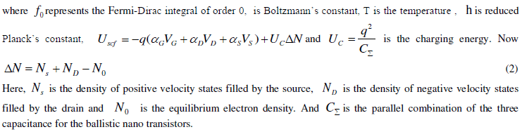
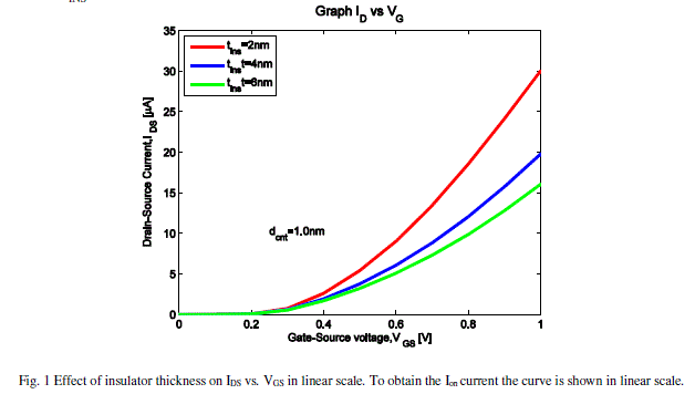
| In this paper, the effect of oxide insulator thickness (tINS)on the CNFET performance is simulated. For simulation, the
CNT diameter (dCNT) is set to 1 nm with the temperature, T is at 300 K, high-k gate dielectric is fixed at k=3.9. Now,the
tINS isvaried from 2-6 nm. Figure 1 shows the plot of drain-source current, IDS vs gate-source voltage,VGSand their
dependence with tINS in linear scale. |
 |
 |
| The figure 1 shows the inverse proportionality of conductivity towards the tINS. Again, if the insulator thickness is small
then the effect of VGS in the CNT would be much greater. Since the modulating of barrier height is controlled by the
VGS, so the conductivity will increase when tINS decreases. For smaller value of oxide thickness, the height of potential
barrier becomes high and tunnelling concept becomes prominent which leads to higher thermionic emission (TE)
current and hence on current is increased [10].On the other hand, figure 2 shows the impact of off current. In this case,
the variance of insulator thickness on the threshold voltage, VTH and off-state current, IDS (OFF) is unchanged and that
leads to the suppression of the ambipolar characteristics. As a result, Ion/Ioff ratio degrades in higher values of oxide
thickness. |
| B.Effect of diameter: |
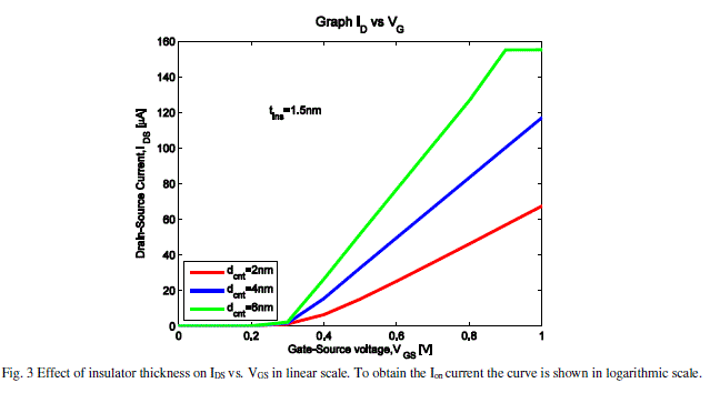 |
| Here, the tINS is set to 1.5nm, while T is at 300K and the diameter dCNT varies from 2-6 nm. Figure 3 shows the ID and
VGS dependence with dCNT in linear scale. The result shows that the conductivity is proportional to the CNT diameter.
The same VTH and IDS for different dCNT is also observed. Due to the proportional characteristics, the IDS conductivity increase enormously with slightly increase in the dCNT. Hence, larger dCNT will give larger current. The valence band
edge of channel is closer to the conduction band edge of the source at the same gate field for lower value of diameter of
CNT. For leakage current increases [10]. As a result on current is increased.
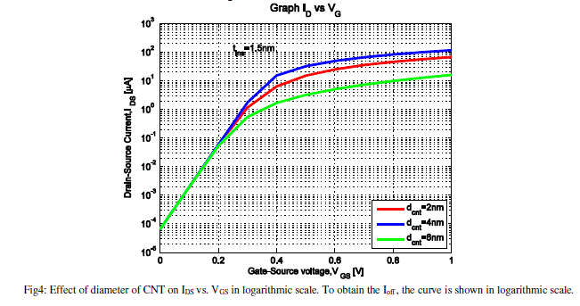
In figure 4, the effect of diameter on the off current is shown. As the off current is very small, the curve is shown in
logarithmic scale. In general, with an increase on the diameter of nano tube, the on current state increased accordingly.
On the other hand, the off state remainsunchanged. |
 |
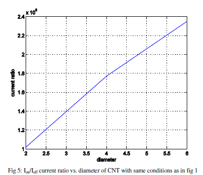
| C. Effect of Ion/Ioff current ratio on CNT diameter and oxide thickness: |
| In this section, for figure 5, the gate oxide thickness is fixed at 1.5nm while the nanotube diameter dCNT is varied from
2-6 nm. Figure 5 presents the Ion/Ioff current ratio as a function of the nanotube diameter. ION is obtained at VGS = 1 V.
IOFF is defined as the current obtained for VGS = 0 V. In both cases, the drain voltage is kept constant at 1 V. It can be
observed that Ion/Ioff currentratio is improved with increase in the nanotube diameter. Using a larger diameter reduces
the band gap, therefore both the onand the leakage current increases rapidly. Thus a significant increase of the Ion/Ioff
ratiois observed with a larger nanotube diameter. So this point must be carefully taken into account to obtain the best
electrical characteristics in perspective to build reliable logic circuits based on CNTFETs. |
 |
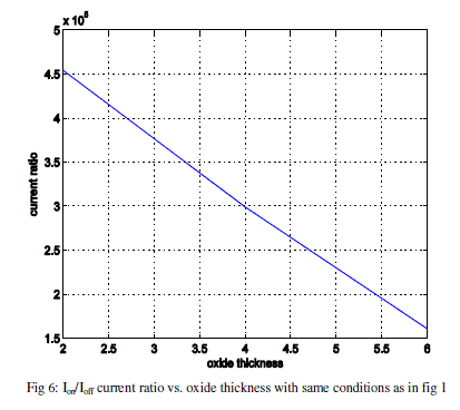
| Now for oxide thickness variation, in figure 6, ION is measured at VDS= 1V and VGS=1V.IOFF defined as the current
obtained for VDS = 1V and VGS=0V. It can be seen from the figure 6 that with decrement of tINS, makes the Ion/Ioff ratio
increases and lead to a high on- state current. This is associated with superior control of the gate voltage over the
channel, which helps in reducing the off- state current. As the on state current largely depends upon the higher energy
level and flow of TE current, it becomes insensitive for device parameter compare to Ioff[10]. |
 |
CONCLUSION |
| Finally it is observed that using large CNT diameter and thinner gate oxide are caused by the enhancement in on-state
current, and off-state current improves in CNTFETs with thinner gate oxide, but they become worse in CNTFETs with
large nanotube diameter.It was observed that the impact of diameter and oxide thickness on the drain current is
noticeable. At the end of these analysis, it shows that both parameters is actually affects the drain current and hence the
performance of ballistic CNTFET. As a conclusion, CNTFET has large potential that can be exploited to be an effective switching device. CNFET is still far to be a commercial device in electronic industry but the researchers are
pushing very hard to improve its performance in order to replace MOSFET as the heart of digital applications. |
ACKNOWDGEMENT |
| The author would like to acknowledge with gratitude to the Dept. of EEE, AUST for providing unfailing support to the
work. |
References |
- R.H. Baughman, A.A. Zhakidov, W.A. deHeer, Science 297, 787 (2002)
- P.G. Collins, P. Avouris, Sci. Am. 283, 62 (2000)
- S. Iijima and T. Ichihashi. Nature, 363:603-605, 1993.
- D. S. Bethune, C. H. Kiang, M. S. Devries, G. Gorman, R. Savoy, and J. Vazquez. Nature, 363:605-607, 1993.
- S.J. Tans, A.R.M. Verschueren, C. Dekker, Nature 393, 49 (1998)
- Thompson, Scott E., and SrivatsanParthasarathy. "Moore's law: the future of Si microelectronics." Materials Today 9.6 (2006): 20-25.
- R. Martel, T. Schmidt, H.R. Shea, T. Hertel, P. Avouris, Appl.Phys. Lett. 73, 2447 (1998)
- K. Alam, R.K. Lake, J. Appl. Phys. 100, 24317 (2006)
- Rahman, A. et. al. âÃâ¬ÃÅTheory of Ballistic Nano transistorsâÃâ¬ÃÂ. IEEE Transactions on Electron Devices, 50(9): 1853-1864 2003
- Shirazi, Shaahin G., and SattarMirzakuchki. "Dependence of carbon nanotube field effect transistors performance on doping level of channel at different diameters: On/off current ratio." Applied Physics Letters 99.26 (2011): 263104-263104.
|