International Journal of Innovative Research in Computer and Communication Engineering
ISSN ONLINE(2320-9801) PRINT (2320-9798)
ISSN ONLINE(2320-9801) PRINT (2320-9798)
Rakhi Saha, Sambita Dalal, Satyasis Mishra
|
| Related article at Pubmed, Scholar Google |
Visit for more related articles at International Journal of Innovative Research in Computer and Communication Engineering
In VLSI applications, area, delay and power are the important factors which must be taken into account which can be minimized by using Reversible logic design. The reversible logic gates are now finding profound as well as promising applications in emerging growing paradigms such as Quantum computing, Quantum Dot Cellular Automata, Optical Computing, Digital Signal Processing, Nanotechnology and etc. This paper presents the novel designs of full adder by using improved reversible logic gates. The main purpose of designing using reversible circuit is to decrease the number of garbage outputs and the number of gates and transistor used.
Keywords |
| Reversible logic; Garbage output; Full adder; Logic gates |
I. INTRODUCTION |
| High-performance chips releasing large amounts of heat impose practical limitation on how far can we improve the performance of the system. Reversible circuits that conserve information, by uncomputing bits instead of throwing them away, will soon offer the only physically possible way to keep improving performance. Reversible computing will also lead to improvement in energy efficiency. Energy efficiency will fundamentally affect the speed of circuits such as nanocircuits and therefore the speed of most computing applications. To increase the portability of devices again reversible computing is required. It will let circuit element sizes to reduce to atomic size limits and hence devices will become more portable. Although the hardware design costs incurred in near future may be high but the power cost and performance being more dominant than logic hardware cost in today’s computing era, the need of reversible computing cannot be ignored. |
| Now a day’s computer scan perform a logic operation for erasing a bit of information. These logic operations are known as irreversible logic. This erasure technique is done in a very inefficiently manner, and which is more than that of energyis dissipated for each bit erased. If we are continue this logic operation in computer hardware performance then we have to reduce the energy dissipated by each logic operation and for improving its efficiency with which we can erase bit. One of the alternative methods is reversible logic. It is the logic that have performed one to one mapping between vectors of inputs and outputs and thus the vector of input states can be always reconstructed from the vector of output states. These logics are known as reversible logic. Even though the use of reversible logic operations are much useful in the designing of systems that needs very little power, this logic provides us an n-Input and n-Output logic function, which has One-to-One Mapping technique because of this technique; we can uniquely determine the output vector from the input vector. |
| The paper is organized as follows: Section II presents the related literature survey. Section III discusses the reversible logic gates. Section IV illustrates our work that is simulation result of full adder using reversible logic and its performance comparison. Section V concludes the paper. |
II. RELATED WORK |
| As per Landauer [1], for irreversible logic, each bit of information lost generates kTln2 Joules of heat energy, where k is Boltzmann's constant and T is absolute temperature at which the computation is performed. For room temperature T, the amount of heat dissipated for one bit is small i.e. 2.9×10⁻²¹ J. The current processors, first of all dissipate 500 times this amount of heat every time a bit is lost. Secondly, assuming every transistor out of more than 4×10⁷ dissipates heat at the processor frequency of 2GHz, the figure becomes 4×10¹⁹*kTln2 J/sec. Bennett [2] showed that if a computation is carried out in Reversible logic zero energy dissipation is possible, as the amount of energy dissipated in a system is directly related to the number of bits erased during computation. The design that does not result in information loss is irreversible. A set of reversible gates are needed to design reversible circuit. Several such gates are proposed over the past decades. Thus Reversibility will become future trend towards for low power dissipating circuit design. In voltage coded logic signal is have energy E=½CV², this energy get dissipated whenever switching occurs in conventional (Irreversibility)logic in CMOS technology. But this form of energy is not lost in Reversible logic design. Hence zero power dissipation is carried out in Reversible logic design [3]. |
III. REVERSIBLE LOGIC DESIGN |
A. Full adder: |
| Full adder is the fundamental building block in many computational units. The anticipated paradigm shift logic compatible with optical and quantum requires compatible reversible adder implementations. The full adder circuit’s output is given by the following equation (1) and (2): |
 |
| The reversible logic implementation of full-adder circuit [8] and other adder circuits and their minimization issues has been discussed further in this paper. |
| B. Basic Reversible logic gates: |
| Reversible logic design differs significantly from traditional combinational logic design approaches. A reversible logic gate is an n-input n-output logic device with one-to-one mapping. This helps to determine the outputs from the inputs and also the inputs can be uniquely recovered from the outputs. Also in the synthesis of reversible circuits direct fan- Out is not allowed as one–to-many concept is not reversible. However fan-out in reversible circuits is achieved using additional gates. A reversible circuit should be designed using minimum number of reversible logic gates. The output lines that are not used further are termed as garbage outputs. One of the most challenging tasks is to reduce these garbage. Quantum cost refers to the cost of the circuit in terms of the cost of a primitive gate. It is calculated knowing the number of primitive reversible logic gates (1*1 or 2*2) required to realize the circuit. Low quantum cost gate design is desirable. |
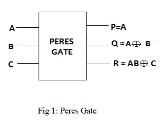
| Peres Gate |
| Fig. 1 shows a 3*3 Peres gate [4]. The input vector is I (A, B, C) and the output vector is O (P, Q, R). Quantum cost of a Peres gate is 4. In the proposed design Peres gate is used because of its lowest quantum cost. |
 |
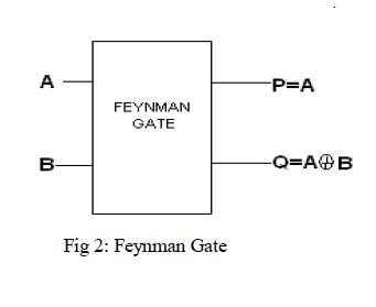
| Feynman Gate |
| Feynman gate is a 2*2 one through reversible gate as shown in Fig. 2[5]. The input vector is I(A, B) and the output vector is O(P, Q). Quantum cost of a Feynman gate is 1. |
 |
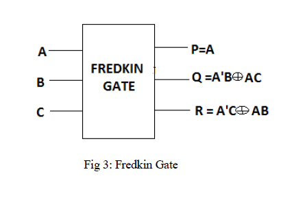
| Fredkin Gate |
| Fig. 3 shows a 3*3 Fredkin gate [6]. The input vector is I (A, B, C) and the output vector is O (P, Q, R). Quantum cost of a Fredkin gate is 5. |
 |
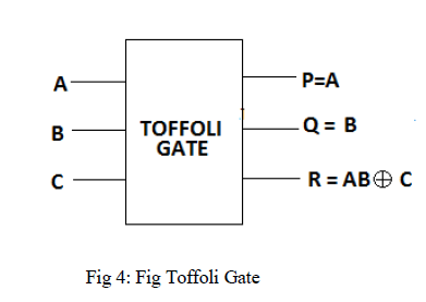
| Fig 4 shows a 3*3 Toffoli gate [7]. The input vector is I (A, B, C) and the output vector is O(P,Q,R).Quantum cost of a Toffoli gate is 5. |
 |
IV. OUR SIMULATION RESULTS |
| Addition is a fundamental operation for any digital system, digital signal processing or control system. A fast and accurate operation of a digital system is greatly influenced by the performance of the resident adders. Adders are also very important component in digital systems because of their extensive use in other basic digital operations such as subtraction, multiplication and division. Hence, improving performance of the digital adder would greatly advance the execution of binary operations inside a circuit compromised of such blocks. The performance of a digital circuit block is gauged by analysing its power dissipation, layout area and its operating speed. |
| Our work consists of Full adder implementation using Peres Reversible gate and Fredkin Reversible gate and their performance measures comparison. The simulation result is obtained in Xilinx ISE simulator using VHDL code and Verilog code. Here the proposed design is compared with the existing Peres Full adder circuit design. |
| A. Full Adder using Fredkin Reversible gate: |
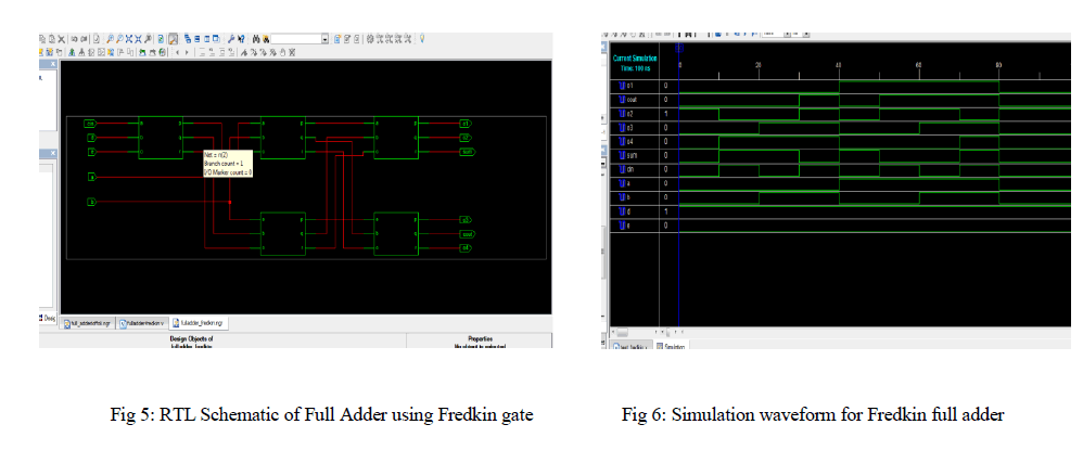
| Full adder can be designed by using five Universal Fredkin gate. Here its input vector are I(a,b,cin,d,e) and its output vector O(o1,o2,o3,o4,Sum and Cout) which is shown in the given Fig.5. Full adder output i.e Sum and Cout can be obtained by making its input as a constant value i.e d=1 and e=0 and its simulation is shown in Fig 6. |
 |
B.Full Adder using Peres Reversible gate: |
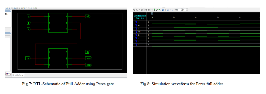
| A full- adder using two Peres gates is as shown in Fig.7.The quantum realization of this shows that its quantum cost is 8 two Peres gates are used. A single 4*4 reversible gate called PFAG gate with quantum cost of 8 is used to realize the multiplier.The simulation waveform of Peres full adder is shown in the given below Fig. 8. |
 |
| C. Performance measure comparison: |
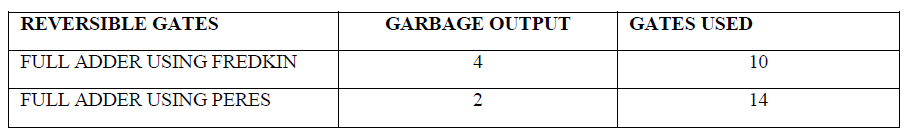 |
| From the above comparisons we can find that mimimum gates is used in full adder using Fredkin reversible gates,hence minimum power dissipation can takes place here. |
V. CONCLUSION AND FUTURE WORK |
| We have designed efficient reversible adder using a novel reversible Peres gate and reversible Fredkin gate. This helps in achieving the reductions in number of reversible gates and garbage outputs. The reversible logic circuits play a very important role in design of low power digital circuits of a future computer. |
| In future quantum cost of each Reversible logic based design can be calculated. Also many more Reversible logic gate types can be used to achieve better performance analysis. Reversible logic gates will be extended to implement more type of combinational and sequential circuit in future. |
References |
|