A compact blind oversampling data-recovery circuit was implemented by using a coarse data-recovery block and an add-drop first-in first out, and it was successfully applied to the universal serial bus (USB)2.0 high-speed packet data transmission. The proposed circuit recovered the serial input data by selecting the sampled data among the 5X oversampled data of a single data bit. It reduced the number of transistors by more than half and the lock time to zero, compared to the conventional blind oversampling data-recovery circuit using the de-multiplexing scheme for multibit-data. The proposed circuit was implemented with a 0.18- m CMOS process. It worked at the data rates ranging from 180 to 720 Mbps. The bit-error rate was measured to be less than 10 -12 with the 215- 1 PRBS data transmitted though a 5-m USB cable. The chip area and the measured power consumption for 480-Mbps operation were 0.185mm2 and 8.2mW, respectively.
INTRODUCTION |
| In the serial data transmission, the data recovery circuit is required because only the data signal is transmitted without
the clock signal to reduce the number of signal wires. The blind oversampling data-recovery circuit is preferred in the
case of universal serial bus (USB), which requires a fast lock time. Since this blind oversampling scheme is a full
digital scheme, it is easier to port into a different process technology than analog scheme and its output jitter is
relatively insensitive to the input data jitter. Also, its lock time is short (less than ten data periods) because of its feedforward
structure. However, it requires a relatively large size first-in first-out (FIFO) and a large peripheral circuitry,
because it needs to store a large size oversampled data in FIFO to locate the accurate sampling time point and process
data in parallel in byte units.[1]–[3] Recently, a hybrid type clock and data recovery (CDR) circuit was proposed[4] to
reduce the FIFO size by combining the analog tracking circuits into the blind oversampling CDR. |
| In this paper, a single-data-bit 5X blind oversampling data-recovery circuit is proposed. The proposed circuit consists
of a 5X oversampler, a coarse data-recovery block, and an add-drop FIFO (AD-FIFO) block. A coarse data-recovery
block recovers the serial input data by selecting the sampled data among the oversampled data of a single-data-bit. This
coarse recovered data may have a missing or duplicate data, which is caused by the input data jitter or the frequency
offset between transmitter and receiver. An AD-FIFO block corrects a missing or duplicate data by adding or removing
a data to and from the FIFO data queue. Compared to the conventional blind oversampling data-recovery circuit using a
de-multiplexing scheme, the proposed circuit reduces the size of FIFO and the peripheral circuitry, and also the lock
time. This proposed circuit was successfully applied to the packet transmission of the USB2.0 high-speed interface
(480 Mbps). |
| In Section II, the architecture of the proposed data-recovery circuit is compared to that of the conventional blind
oversampling data-recovery circuit. In Section III, the operation of coarse data-recovery block is shown. The structure
and the operation of AD-FIFO are presented in Section IV. In section V, the measurement results are presented,
followed by the conclusion in Section VI. |
ARCHITECTURE |
| A. Conventional Blind Over sampling Data-Recovery Circuit |
| The blind oversampling technique was used as a timing recovery technique in the universal asynchronous receiver/ -
transmitter (UART). Recently, this technique was adopted to the serial link.[2] In this technique, the serial input data
are oversampled using the multiphase clocks, and the
recovered data are generated by using the de-multiplexing scheme. |
| Fig. 1(a) shows an application of this technique to the USB receiver. The serial input data are 3X oversampled by the
24 multiphase clocks. The 24-bit oversampled data are aligned to the receiver clock and transferred to both FIFO1 and
the edge detector at the same time. The edge detector finds the transition of input data by XOR-ing the two sampled
data adjacent in time. The voter accumulates the number of data transitions during each time interval between the
multiphase clocks and determines one of the multiphase clocks to be the sampling phase by using the majority voting
scheme. It takes several data periods for the voter to determine the sampling phase and the sampled data. During this
time interval, all the oversampled data must be stored in FIFO1. |
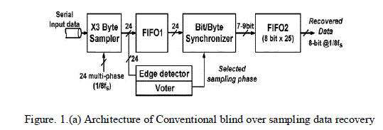 |
| The frequency offset between transmitter and receiver may induce errors in the recovered data. To compensate for
errors, the bit/byte synchronizer sends out 7, 8, or 9 bits in parallel to FIFO2 and FIFO2 packs the incident data into 8-
bit units and sends out the packed 8-bit data as the recovered data. The conventional blind oversampling scheme
requires a relatively large circuit because of the de-multiplexing architecture of converting the 1-bit serial input data
into the 8-bit parallel recovered data. The data-recovery circuit of Fig. 1(a) has a lock time of several data periods
because of the insufficient accumulation of data transition information at the beginning stage of data-recovery process. |
| B. Proposed Blind Oversampling Data-Recovery Circuit |
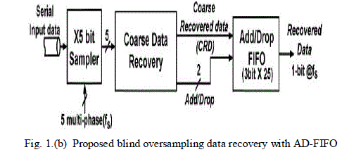
| Fig. 1(b) shows the proposed data-recovery circuit, which uses the five multiphase clocks with the same nominal
frequency (f s ) as the serial input data rate. The coarse data-recovery block recovers a coarse data bit from the 5-bit
over sampled data which corresponds to a single data bit. Because of this arrangement, FIFO1 of Figure 1 is removed
and the logic circuitry to determine the sampling phase is simplified in the proposed circuit. With the frequency offset
between transmitter and receiver or the input jitter, the coarse data-recovery circuit may generate some missing or
duplicated data, which are corrected by the following AD-FIFO. AD-FIFO is a modified FIFO, where a data bit can be
dropped from or inserted into the FIFO queue while it follows the FIFO sequence. |
 |
COARSEDATA-RECOVERY BLOCK |
| A. Block Diagram |
| The block diagram of the coarse data-recovery block is shown in Figure 2.(a) |
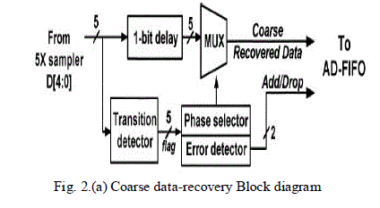 |
| It accepts the 5-bit data (D [4:0]) from the 5X sampler as input, and generates the 1-bit coarse recovered data (CRD)
and the Add/Drop signals as output. The transition detector finds the time interval of input data transition out of the five
time intervals between the adjacent multiphase clocks, by using the current 5-bit oversampled data (D [4:0] ) and the
previous 1-bit oversampled data (D’[0]). It sends out the 5-bit flag data to both the phase selector and the error detector.
The phase selector determines the sampling phase from the 5-bit flag data. It maintains the previous sampling phase if
the 5-bit flag data is all zero, which indicates no transition in the input data. The 5-to-1 multiplexer (MUX) selects the
1-bit data corresponding to the sampling phase determined by the phase selector, among the 5 oversampled data input.
It sends out the selected sampled data as the (CRD). The 1-bit delay block compensates for the time delay of the
transition detector to synchronize the oversampled data to the selected sampling phase at the MUX. The error detector
compares the current and previous values of the 5-bit flag data and generates Add/Drop the signals. |
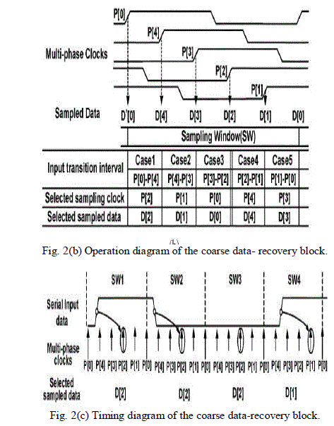
| B.Center Picking Method Within a Single Sampling Window |
| Fig. 2(b) shows the center picking method within a single sampling window. This method is used by the coarse datarecovery
block of this work to determine the sampling phase and the sampled data, depending on the transition position
of input data (Case1-5). The sampling window (SW) is defined to be a time period starting from one rising edge to the
following rising edge of the P[0] clock which is one of the 5 multiphase clocks. The coarse data-recovery block accepts
the 5-bit oversampled data of a single sampling window, and finds the transition position of input data. Then, it
determines the sampling phase and the sampled data within the same sampling window.
For example, in the Case1, where the input data changes in between the rising edges of P[0] and P[4], the following
P[2] phase in the same sampling window is selected as the sampling phase because the center point (max. data eye
point) of input data is located around the rising edge of P[2] clock. Therefore, this scheme is called the center picking
method within a single sampling window. Since this scheme requires the data transition information only within a
single sampling window, it reduces the hardware by removing the FIFO1 and the voting logic of the conventional
scheme. |
| Fig. 2(c) shows the timing diagram of the coarse data-recovery block. If the data transition position always belongs
to one of the three cases (Case1-3) continuously in time, the third phase after the data transition (P[2],P[1],P[0]) is
chosen as the sampling phase. If the data transition position always belongs to one of the two cases (Case4-5)
continuously in time, the third phase before the data transition (P[4],P[3]) is chosen as the sampling phase. These two
groups of cases ensure the normal data recovery without any errors. |
 |
| C. Correction of Missing Or Duplicate Data |
| If there is a frequency offset between transmitter and receiver, the input data transition position moves in the forward
or back ward direction monotonically with time in a sampling window. Eventually it will hit the sampling window
boundary. In this case, the missing or duplicate data will occur in the CRD, and the coarse data-recovery block
activates the Add/Drop signals, which are sent to the following AD-FIFO block, as shown in Fig.1(b) |
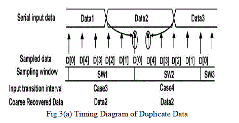 |
| When the transmitter frequency is higher than the receiver frequency, the duplicate data will appear in the CRD. In
Fig.3(a), the input data transition belongs to the Case3 during the sampling window SW1 and the Case4 during the
following sampling window SW2. During SW1, the third phase (P[0]) after the data transition is selected as the
sampling phase and Data2 is recovered as CRD. During SW2, the third phase (P [4]) before the data transition is
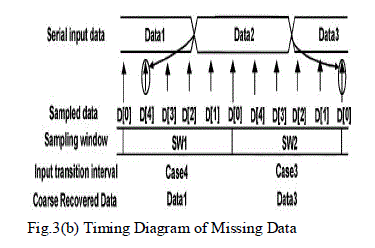
selected as the sampling phase, the same Data2 as in SW1 is recovered as CRD.When the receiver frequency is higher
than the transmitter frequency, the missing data will occur in the CRD. Fig.3(b) shows one of these cases. The input
data jitter may also induce the missing or duplicate data in CRD. |
 |
| To resolve the problem of missing or duplicate data, the error detector within the coarse data-recovery block
activates the Add or Drop signal, synchronized to CRD, as shown in Fig. 3(c). The Add/Drop signals are activated only
during a single clock cycle after the particular change of the selected sampling phase. When there is no transition in the
input data, the Add/Drop signals are not activated because the selected sampling phase retains the previous value. The
AD-FIFO block receives the CRD and Add/Drop signals, and recovers the correct data by adding the missing bit or
removing the duplicated bit in the data queue. |
AD-FIFO BLOCK |
| A.Operation Of AD-FIFO Block |
| The AD-FIFO block performs the basic FIFO operation. However, it can add or remove a single bit to or from the
data queue by the control of the Add or Drop signal. Fig.4(a) shows the block diagram of the AD-FIFO block with 2N
+ 1AD FIFO cells. The number of AD-FIFO cells is determined by the given maximum packet size and the frequency
offset between transmitter and receiver. The maximum packet size is given by the interface standard, for example, it is
8255 bits in the USB standard. The CRD and Add/Drop signals of an AD-FIFO cell are shifted to the next right ADFIFO
cell at every rising edge of clock. Fig.4(b) shows the block diagram of an AD-FIFO cell. Each cell has a tri-state
buffer at output and all the output nodes (CO) of all the AD-FIFO cells are connected to a single node RD, which is the
output node of the AD-FIFO block. |
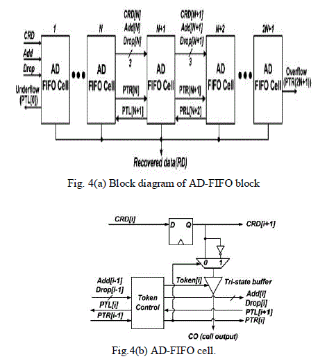 |
| Only the tri-state buffer of a single AD-FIFO cell is enabled among those of the 2N + 1 cell by using a token signal
(Token[i]). Only the token signal of a selected cell is set to 1 with those of all the other 2N cells set to 0. An AD-FIFO
cell passes the token signal to the left or to the right by activating the Pass Token to the Left (PTL) or Pass Token to the
Right (PTR) signals. When there is a missing bit, the token signal is passed to the right. When there is a duplicate bit,
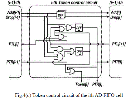
the token signal is passed to the left. Fig.4(c) shows the token control circuit of the ith AD-FIFO cell. The upper two D
F/Fs form the shift registers to synchronize the Add and Drop signals to the CRD signal. The lower two D F/Fs form a
one-stage pipe-line to maximize the operation clock frequency by minimizing the time delay of the Token[i] and
PTR[i] signals from the clock rising edge. |
 |
| The one-clock latency caused by the one-stage pipeline is compensated for by using the prediction logic with the
preceding cell output as input. |
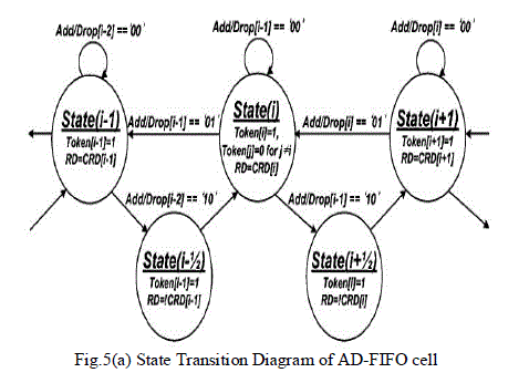 |
| Fig.5(a) shows the state transition diagram of the entire AD-FIFO block. The State (i) represents the state where the
token signal of the ith cell (Token[i]) is set to 1 with those of all the other cells set to 0. If the AD-FIFO block is in the
State (i) and there is a duplicated bit, the Drop [i-1] signal is activated to 1. Then the AD-FIFO block change to the
State (i-1) at the next rising edge of clock, and RD (output of the AD-FIFO block) is set to CRD [i-1] output of the (i-1)
th cell. In this way, the token moves to the left adjacent cell in one clock period, and the duplicated bit is eliminated in
the recovered data (RD). |
| If there is a missing bit, the Add [i-1] signal is activated to 1. Then, the AD-FIFO block changes to the State (i+1/2)
at the next rising edge of clock, and RD is set to! CRD[i] (the inverted value of the th cell output). At the following
rising edge of clock, the AD-FIFO block changes to the State (i+1). In this way, the token moves to the right adjacent
cell in two clock periods, and the missing bit (! CRD[i]) is added in RD at the State (i+1/2). After that, the normal data
recovery is continued with RD connected to the output of the (i+1)th cell. The! CRD[i] is added to RD for the missing
bit, because the missing bit CRD[i] (DATA2 of Figure 7) is the inverted value of the following data [DATA3 of Figure
3.4 This is because the missing bit occurs after the change of the selected sampling phase and the selected sampling
phase changes with the input data transition, the missing bit always occurs just after the input data transition |
| In Fig.5(b), the operation of the AD-FIFO block is presented in the form of timing diagram. Assume that the ADFIFO
block is initially in the State (i), where the ith cell is selected by the token signal to be the output cell which sends out CRD[i] as RD. When there is no Add or Drop signal activated, as shown for the first four data (D0 – D3) of
Fig.5(b), the AD-FIFO block remains in the State (i) and the ith cell sends out CRD[i] as RD at the next rising edge of
clock. When there is an Add signal activated (AD4), the AD-FIFO block changes to the State (i+1/2) at the next rising
edge of clock and the ith cell sends out! D4 as RD. After that, the AD-FIFO block changes to the State (i+1) at the next
rising edge of clock and sends out D4 as RD. This case corresponds to the transition of the selected sampling phase
from Case4 to Case3, as shown in Fig.3(b). |
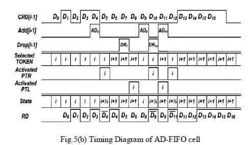 |
| When there is a Drop signal (DR7) activated, the AD-FIFO block changes to the State(i) at the next rising edge of
clock and it skips D7, which is the data signal synchronized to the Drop signal (DR7), This case corresponds to the
transition from Case3 to Case4, as shown in Fig.3(a). The successive occurrence of Add, Drop and Add signals (AD9,
DR10, AD11) indicates the worst case of input data jitter, where the selected sampling phase changes from Case4, to
Case3 and back to Case4. Even in this case, the correct data sequence of! D9, D9,! D11, D11 appears in RD, as desired. |
CONCLUSION |
| A single-data-bit blind oversampling data-recovery circuit is proposed. It consists of a 5X oversampler, a coarse
data-recovery block, and an AD-FIFO. The coarse data-recovery block operates on a single sampling window, which
consists of 5 oversampled data corresponding to a single-data bit. It generates a coarse recovered data. The AD-FIFO
corrects any missing or duplicated data in the coarse recovered data, and generates the final recovered data. The coarse
data-recovery block reduced the number of transistors by more than half and the lock time to zero, compared to the
conventional blind oversampling data recovery using the de-multiplexing scheme for 8-bit-data. The AD-FIFO
performs the correct data recovery even with the frequency offset between transmitter and receiver or the input data
jitter, by adding or removing a data bit to and from the data queue. |
References |
- Kim .J and Jeong .D.K, âÃâ¬ÃÅMulti-gigabit-rate clock and data recovery based on blind oversampling,âÃâ¬Ã IEEE Commun. Mag., vol. 41, no. 12, pp. 68âÃâ¬Ãâ 74, Dec. 2003.
- Lee .K, Kim .S, Ahn .G, and Jeong .D.K, , âÃâ¬ÃÅA CMOS serial link for fully duplexed data communication,âÃâ¬Ã IEEE J. Solid-State Circuits, vol. 30, no. 4, pp. 353âÃâ¬Ãâ364, Apr. 1995.
- Yang . C, R. Farjad-Rad .R, and Horowitz .M, âÃâ¬ÃÅA 0.5 um CMOS 4.0 Gbit/s serial link transceiver with data recovery using oversampling,âÃâ¬Ã IEEE J. Solid-State Circuits, vol. 33, no. 5, pp. 713âÃâ¬Ãâ722, May 1998.
- Van Ierssel .M, Sheikholeslami .A, Tamura .H, and Walker .W, âÃâ¬ÃÅA 3.2 Gb/s semi-blind-oversampling CDR,âÃâ¬Ã in ISSCC Dig. Tech. Projects, Feb. 2006, pp. 334âÃâ¬Ãâ335.
- âÃâ¬ÃÅUSB2.0 Transceiver Macrocell Interface Specification, Revision 1.05,âÃâ¬Ã Intel, Hillsboro, OR, Mar. 29, 2001.
|