International Journal of Advanced Research in Electrical, Electronics and Instrumentation Engineering
ISSN ONLINE(2278-8875) PRINT (2320-3765)
ISSN ONLINE(2278-8875) PRINT (2320-3765)
Nemitha B1 and Pradeep Kumar B.P2
|
| Related article at Pubmed, Scholar Google |
Visit for more related articles at International Journal of Advanced Research in Electrical, Electronics and Instrumentation Engineering
One of the important functional blocks in frequency synthesizers is the high speed dual modulus prescaler. Prescaler determines how fast the frequency synthesizer is. The bottleneck of the dual modulus prescaler design is that it operates at the highest frequencies and consumes more power than any other circuit blocks of the synthesizer. Reduction of power consumption and delay is very important for high speed low power applications. This paper gives an idea about the different techniques that are used to reduce the power consumption and avoid delay of prescaler. The different approaches towards design of N/(N+1) prescaler using true single phase clock(TSPC) flip-flop and Extended true single phase clock (ETSPC) flip-flop and different logic gates are embedded between the flip-flops to achieve two ratios and also to reduce the switching power and short circuit power in the prescaler is analyzed.
Keywords |
| Dflip-flop (DFF), true single phase clock (TSPC), Extended true single phase clock (E-TSPC). |
INTRODUCTION |
| CMOS has been the main technology for very-large-scale integration (VLSI) system design. From the beginning to nowadays, several CMOS clock policies have been proposed. One of the critical functional blocks in frequency synthesizers is the high speed dual modulus prescaler. It operates at the highest frequencies and consumes more power than any other circuit blocks of the frequency synthesizer. Hence the design of dual modulus prescaler is so crucial. A dual modulus prescaler usually consists of a divide-by-2/3 prescaler unit followed by several asynchronous divide-by-2 units. |
| In general a divide-by-N/N+1 counter consist of flip flops and some extra logic implemented using logic gates. Various flip-flop based designs have been proposed to improve the operating speed of dual-modulus prescalers. These designs suffer from large load capacitance which limits the maximum operating frequency which in turn increases the power consumption. Therefore, dynamic and sequential circuit techniques or clocked logic gates such as, True Single Phase Clocks (TSPC) have to be used to reduce the circuit complexity, power dissipation and increase the operation speed. |
| TSPC logic based designs can be further enhanced by using the Extended True Single Phase Clock (E-TSPC) logic. E-TSPC logic based designs are more suitable for high speed and low power applications. The counting logic and the mode selection control are implemented using different techniques. So this eventually reduces the power consumptions and hence the operating frequency also increases. |
| A survey of different existing prescaler designs which include both TSPC and E-TSPC based designs are, instead of an AND and an OR gate two NOR gates are used [1] this reduces the switching nodes. Two AND gates are used in the place of AND and OR gate [2] .A single AND gate is used in common as switch [3].the transmission gate is used as logic gate [4]. All these techniques are different approaches to reduce the power, delay and area of prescaler circuit. |
RELATED RESEARCH |
| In this paper the power consumption and operating frequency of true single phase clock (TSPC) and extended true single phase clock (E-TSPC) frequency prescalers are investigated. Based on this study a new low power and improved speed TSPC 2/3 prescaler is proposed which is silicon verified. Compared with the existing TSPC architectures the proposed 2/3 prescaler is capable of operating up to 5 GHz and ideally, a 67% reduction of power consumption is achieved when compared under the same technology at supply voltage of 1.8 V This extremely low power Consumption is achieved by radically decreasing the sizes of transistors, reducing the number of switching stages and blocking the power supply to one of the D flip-flops (DFF) during Divide-by-2 operation [1]. |
| In this paper the short-circuit power and the switching power in the E-TSPC-based divider are calculated and simulated. A low-power divide-by-2/3 unit of a prescaler is proposed and implemented using a CMOS technology. Compared with the existing design, a 25% reduction of power consumption is achieved [2]. |
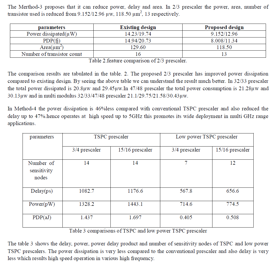
| In this paper the E-TSPC logic based divide-by-2/3 prescaler suitable for low supply voltage (0.9V) and low power applications is been designed and implemented wherein the counting logic and the mode selection control are implemented using a single transistor. Thus the critical path is reduced which in turn enhances its working frequency. Compared with the conventional TSPC and E-TSPC based 2/3 prescaler designs as much as 46% in PDP, 24% in operation speed and 44% in area can be achieved by the proposed design. Also a 32/33 prescaler, 47/48 prescaler and a multi modulus 32/33/47/48 prescaler which incorporates the proposed 2/3 prescaler are designed and implemented [3]. |
| In this paper True Single Phase Clock (TSPC) based on Ratio logic D flip-flop and Transmission Gates (TGs) is implemented in 0.18μm CMOS process. A Glitch elimination TSPC D-flip flop is used in the synchronous counter. TGs are used in the critical path and the control logic for mode selection. The power efficient TSPC design technique is applied to 3/4 and 15/16 prescalers, and their performances are compared. Simulation and measurement results show high-speed, low-power, low PDP and multiple division ratio capabilities of the power efficient technique with a frequency range of 0.5-3.125GHz. The improved speed, the power efficiency, and the flexibility will promote its wide deployment in Multi gigahertz range applications [4]. |
METHODOLOGY |
A. METHOD-1 |
| This method has two new designs of TSPC 2/3 prescaler .design-I is improved TSPC 2/3 prescaler and design-II is ultra low power TSPC 2/3 prescaler [1]. |
| The improved TSPC 2/3 prescaler has improved speed and low power dissipation. This design consist of two DFlip- flop and two NOR gates instead of an AND gate and an OR gate in between the flip-flops. This design-I is as shown in the figure.1 |
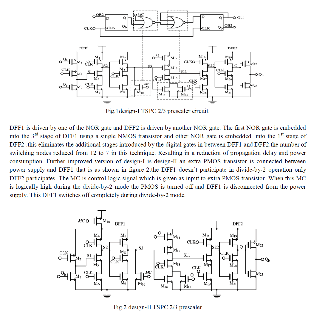 |
| When the MC is logically low the PMOS transistor is turned on and supplies power to DFF1 and divide-by-3 operation performs. |
B. METHOD-2 |
| In this method the E-TSPC based prescaler is proposed in different technique to avoid unnecessary power consumption. In this method two AND gates are used instead of one OR gate and one AND gate to achieve a 2/3 prescaler with minimal power consumption. This is as shown in the figure 3.when the MC is logically high it control the NMOS and when MC is logically low it control the PMOS. When MC is high the DFF1 is blocked so the nodes in the DFF1 are blocked. And only 1st stage has the short circuit path and the remaining stages have no switching activities or short circuit while DFF2 performs divide-by-2 operation. The power consumption is also reduced during the divide-by-3 operation due to complementary logic type and also due to less short circuit power consumption in DFF1. |
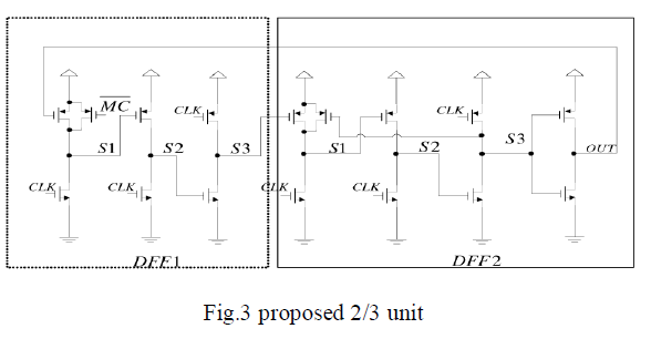 |
C. METHOD-3 |
| This technique consists of two flip-flops and single AND gate in common. The division control logic is implemented using a switch. When the switch is open the input from FF1 is disconnected and the FF2 alone performs divide-by-2 operation when the switch is close. The FF1 and FF2 are linked to form a counter with three distinct states and thus perform divide-by-3 operation. This is as shown in the figure4. |
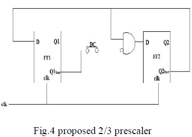 |
| The E-TSPC FF design remains intact without any logic embedding so that the effect of parasitic capacitance is alleviated .the inverter to complement the one of the two E-TSPC FF outputs for divide-by-3 operations is removed using these techniques a 32/33 prescalar,47/48 prescaler and multi modulus 32/33/47/48 prescaler are designed. |
D. METHOD-4 |
| In this method a 3/4 prescaler extends the output by one cycle in every two cycles .The 3/4 prescaler removes one cycle in every 4 cycles by comparing the outputs of the two D-flipflops. It improve the speed and reduce power consumption. The critical path delay is primarily due to the delay of logic gates used for mode selection .this technique is as shown in the figure 5.in this technique the transmission gates are used as logic gates and control logic for mode selection .it has a higher speed by eliminating the NOR gate which introduced critical path delay as well as lower power consumption by minimizing the number of full speed DFFs in the 1st stage. The MUX used is a two input path selector which selects different modes depending upon the control signal. |
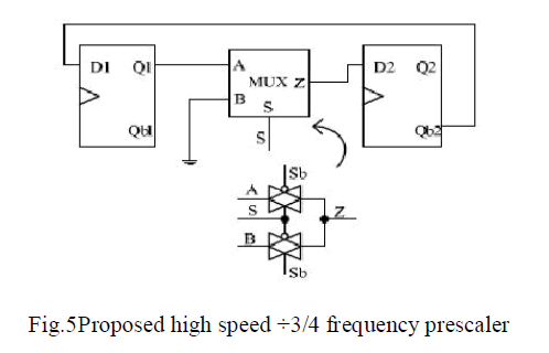 |
RESULTS |
| In Method-1 the switching power is reduced up to 42%and speed is improved by 1.3 times than the conventional circuit since the reduction of number of stages the short circuit power also reduced. The figure 6 shows the power consumption by design-I and design-II. |
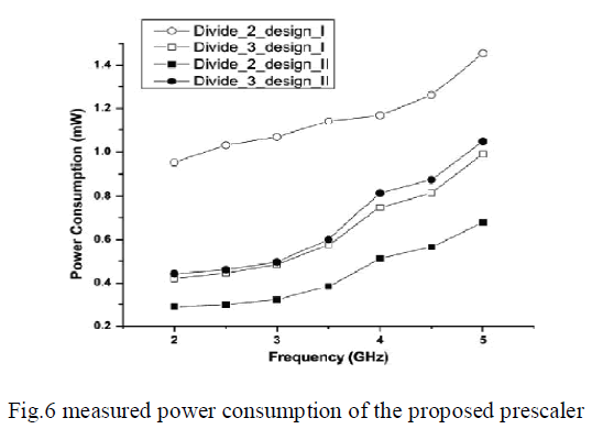 |
| The power consumption in the divide-by-2 mode is double than the power consumed in the divide-by-3 mode.the design-II completely removes the short circuit power and switching power of DFF1the maximum frequency of operation is improved in design-II and is almost same as that of the design-I[1]. |
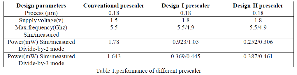 |
| The table 1 shows that performance of different prescaler.the conventional prescaler is compared with the proposed design-I and design-II[1].the different design parameters are process,supply voltage,maximum frequency and power are tabulated. |
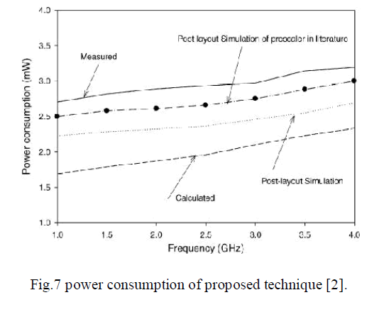
| In Method-2 the E-TSPC based proposed technique has approximately 10%lower power consumption in the divideby- 3 operation and lessthan 40%of the power consumption in the divide-by-2 operation due to reduced switching activities and short circuit in DFF1.the figure 7 showes the power consumption of the proposed technique[2].if two operation are equal probability in the dual modulus prescaler a 25%reduction in the power consumption is achived with an input of 4.5 GHz. |
 |
 |
CONCLUSION |
| In this paper, the concept of different methodologies that are used to improve the performance of the prescaler has been discussed. They have demonstrated new various approaches to reduce the power dissipation of prescaler circuit using TSPC and E-TSPC flip-flops. Each method has better improvement than that of conventional design. Instead of using an OR gate and AND gate in between FFs they used different logic gates such as NOR gates, AND gates, transmission gates and transistors to achieve high speed of operation with less power consumption. The E-TSPC logic [3] which has discussed in this paper has better performance and lesser power consumption and reduces numbers of transistor by using a single PMOS transistor in between FFs rather than using logic gates. |
References |
|