Keywords
|
| Electronic ballasts, Flyback converters, Lighting, Power factor correction (PFC). |
INTRODUCTION
|
| Electronic ballast is a device which uses solid state electronic circuit to control the starting voltage and operating currents of lighting device. It usually supplies power to the lamp at a frequency of 20 KHz or higher which eliminates the stroboscopic effect of flicker. By using electronic ballast, the efficiency and life of the lighting system can be improved. Light emitting diode (LED) sources are more compact, less dissipative and more durable, are finding more applications in domestic, commercial and industrial environments. |
| The block diagram of electronic ballast for lighting systems is shown in Fig 1(a). First stage is the diode bridge rectifier stage to convert AC (alternating current) to DC (Direct current). The rectifier stage is connected to the input power factor correction (PFC) stage. The input PFC stage supplies a capacitor which provides constant voltage across the output stage. The output stage is a DC-DC converter stage, used to supply lighting systems. |
| The block diagram of proposed scheme stages for lighting systems is shown in Fig 1(b). It consists of a Bidirectional input stage consisting of two Flyback converters with different polarities, in order to avoid the use of the diode bridge rectifier stage. The input stage supplies a capacitor, which provides constant voltage across the output stage. The output stage is a boost converter which supplies the lighting systems. |
LITERATURE SURVEY
|
| In the literature, many topologies have been used for this input stage, which have some drawbacks. For example, the use of bridgeless high power factor buck converter as the input stage, although minimizes the number of conducting semiconductor components, works as a voltage doubler. As the output voltage is doubled, the switching losses of the primary switches of the output stage increases. Therefore, if an isolated input stage is used, the output voltage bus value can be made lower. The paper mainly deals with the use of Bidirectional flyback topology, to eliminate the use of diode bridge rectifier in order to improve the efficiency. |
INPUT PFC STAGE
|
| The PFC power topology presented in the paper is based on the integration of two flyback converters, one for each polarity of the line voltage, thereby completely eliminating diode bridge rectifier and avoiding the losses of input diode bridge rectifier. Here, the discontinuous conduction mode of the flyback is considered. The proposed topology is shown in the Fig. 2 |
A. Operation under Positive Input voltage
|
| The operation can be explained in two modes |
| Mode 1: This mode begins when switch M1 is turned ON. When the switch M1 is turned ON, the input line voltage Vac is applied across the first primary winding of the transformer. The current through the primary inductor and switch increases with a rate of Vac/ LP where LP is the inductance as seen from the primary. The magnetizing inductance of the transformer begins to charge during this period. From Fig 3(a), the diode D1 is reverse biased and therefore no current flows through the secondary winding connected to D1. |
| Mode 2: This mode begins when switch M1 is turned OFF. The magnetizing inductance discharges through the secondary side of the transformer, and the polarity of the winding reverses. The diode D1 results in forward bias as shown in Fig 3(b). The stored inductor energy now flows through the secondary diode and into the capacitor and the load. The rate of this current is Vac/ LS where LS is the inductance as seen from the secondary.Once the magnetizing inductor of the flyback transformer is fully demagnetized, the diode D1 results in reverse biased and no current flows through the transformer. |
B. Operation under Negative Input voltage
|
| The operation can be explained in two modes |
| Mode 1: This mode begins when switch M2 is turned ON. When the switch M2 is turned ON, the input line voltage Vac is applied across the second primary winding of the transformer. The current starts to build up and the magnetizing inductance of the transformer begins to charge. During this mode, the diode D1 is reverse biased as shown in Fig. 4(a) and therefore no current flows through the secondary winding of the transformer. |
| Mode 2: This mode begins when switch M2 is turned OFF. The magnetizing inductance discharges through the secondary side of the transformer, and the polarity of the winding reverses. The diode D1 becomes forward biased as shown in Fig 4(b) and current flows through the secondary winding connected to diode D1. Once the magnetizing inductor of the flyback transformer is fully demagnetized, the diode D1 results in reverse biased and no current flows through the transformer |
DESIGN DETAILS OF THE INPUT STAGE FOR 50W LED LAMP
|
| The design inputs for input flyback stage are given in this section. |
 |
 |
 |
 |
 |
 |
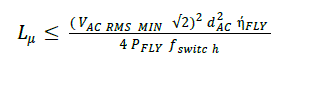
| Where ηFLY is the estimated efficiency of the flyback stage, fswitch is the switching frequency of the flyback stage, VAC RMS is the RMS value of the line input voltage, dAC is the duty ratio of the input flyback stage, PFLY is the required power output of the flyback stage, PLED is the load power, ÎîOUT is the output stage efficiency. |
| The magnetizing inductance of the flyback converter can be given as |
 |
| Substituting the values in equation 7, |
| ïÿýïÿýïÿýïÿý ≤ 172 μïÿýïÿý |
| During Mode 2, the stored inductor energy transferred to the capacitor has to supply power ïÿýïÿýïÿýïÿý to the load and also to replenish the energy lost by the capacitor during the previous Mode (Mode 1). Thus, |
 |
| Where Ts is the switching period of the input flyback stage, Ls is the inductance as seen from the secondary, Is is the current flowing through the secondary side of the transformer |
 9) 9) |
 |
| To calculate ïÿýïÿýïÿýïÿý+ :- |
| Desired power output of flyback stage PFLY = 55W (11) |
| Desired output voltage of flyback stage, V = 70 V (12) |
Load Resistance of flyback stage  |
Output current of flyback stage,  |
| Where V is the required output voltage of the flyback stage, P is the required power output of the flyback stage. From the circuit shown in the Fig. 2. |
| Diode current IS+ = Capacitor current + Resistor current (15) |
| Assuming output capacitor ïÿýïÿý = 47μïÿýïÿý (16) |
| Hence ïÿýïÿýïÿýïÿý+ = 1.81 ïÿýïÿý (17) |
| ïÿýïÿýïÿýïÿý = 335 μïÿýïÿý (18) |
 |
| 1100 ïÿýïÿýïÿýïÿý (20) |
| Where LP1 and Lp2 are the inductances as seen from the primary. |
OUTPUT STAGE
|
| The CCM Boost converter is used as the output stage. The switching frequency considered is 100 KHz. The Circuit diagram of the Boost converter (output stage) is as shown in the Fig 5. When the MOSFET is turned ON, the inductor current rises and energy is stored in the inductor. If the MOSFET is turned OFF, the energy stored in the inductor is transferred to load (LED). |
| Input voltage VIN = 70V |
| Required output voltage = 140V |
| For Boost converter, |
 |
| By substituting the values of VO and VIN , the duty ratio of the boost converter is 0.5 |
| Target power output of the boost converter W = 50ïÿýïÿýïÿýïÿýïÿýïÿýïÿýïÿýïÿýïÿý (22) |
Output current of the boost converter  |
Load resistance of the boost converter |
The value of boost inductor,  |
| The value of the boost capacitor is calculated considering 10% output ripple voltage |
 |
| Where R is the load resistance and f is the switching frequency of the boost converter |
SIMULATION RESULTS OF THE PROPOSED CONVERTER
|
A. Simulation results of the proposed input stage
|
| The simulink model of the proposed input stage is shown in Fig 6. In the model, the simulation parameters for Lp1 and Lp2 are set to 1100 μH, LS = 335μH, C= 47μF. |
| The gate pulses required for MOSFETâÃâ¬ÃŸs M1 and M2 are obtained by comparing the sinusoidal waveform (reference signal) with the repetitive triangular waveform ( carrier signal) in the relational operator block and the required pulses are generated at the output of the relational operator block as shown in Fig. 6. These gate pulses are needed to turn on MOSFET„s M1 and M2 alternatively i.e during positive cycle of the applied voltage, the MOSFET M1 is turned ON and during negative half cycle, the MOSFET M2 is turned ON. The gate pulses given to MOSFETs M1 and M2 connected in the primary winding of the Flyback transformer is shown in Fig 7(a) and 7(b) respectively. The output voltage and current waveforms of Flyback stage is shown in Fig 7(c) and Fig 7(d) respectively |
| The voltage magnitude required for output stage is 70 V, and the same is obtained at the output of the input flyback stage. From Fig. 7(c), it is evident that the required voltage of 70 V (steady state value) is obtained across the load resistance of the flyback stage and the same is applied to the output stage. Further, from Fig. 7(d), it is clear that the output current of 0.73A (steady state value) is obtained in order to get the desired output power. |
B. Simulation Results of the output stage
|
| The output voltage of 70 V which is obtained from input flyback stage is applied to the input terminals of the output stage. The SIMULINK model of the output stage (Boost converter) is shown in Fig. 8. The boost converter is needed to step up the voltage from 70V to 140V. The MOSFET in the output stage is turned ON and turned OFF with a switching frequency of 100 kHz. An output capacitor is used to reduce the ripple in the output voltage. The output voltage waveform of the Boost converter is shown in Fig.9. From Fig. 9, it is observed that the input voltage 70V is increased to 140V which is desired voltage required to supply LED lighting system. |
| The complete simulink model of the proposed converter i.e along with input flyback stage and output stage is shown in Fig 10. From Fig. 10, it is clear that the complete setup has got two stages which are cascaded. |
LOSSES AND EFFICIENCY OF THE PROPOSED CONVERTER
|
| The various losses i.e conduction and switching losses of different components used in the proposed converter are determined from the practical considerations and are depicted in Table I. |
| From Table-1, it is clear that the total conduction losses across the diodes and MOSFET are 1.37 mW and 39.6 mW respectively. Further it is observed that the conduction losses occurred across the switching devices is less than the losses that are occurred across the secondary winding of the transformer. Moreover, the switching losses are found to be about 1.2 W. |
| Efficiency Îî = (Power Output/ power input) X 100 = 93.05% |
| The conduction and switching losses of the proposed converter and converter [1] is given in Table II. From Table-II, it is clear that the conduction and switching losses of the proposed converter is lower than the losses of converter topology [1]. Hence, the efficiency of the proposed converter is higher than the converter [1]. Table III gives the efficiency of the proposed converter and converter [1]. |
CONCLUSION
|
| An efficient electronic driver for lighting application has been designed and presented in this paper. The design for the proposed converter has been carried out for a 50 W LED lamp. The proposed converter circuit is designed and tested through SIMULINK. The efficiency and losses of the proposed converter are calculated using simulation results and it is found that the proposed converter configurations gives better efficiency as compared to the other converter topologies that has been presented in the literature. In the proposed converter, the number of switching components is minimized when compared to the other converter configurations. Hence the conduction and switching losses are minimised and thereby increasing the efficiency of the converter. |
Tables at a glance
|
|
|
Figures at a glance
|
 |
 |
 |
 |
 |
| Figure 1 |
Figure 2 |
Figure 3 |
Figure 4 |
Figure 5 |
 |
 |
 |
 |
 |
| Figure 6 |
Figure 7 |
Figure 8 |
Figure 9 |
Figure 10 |
|
References
|
- Garcia, D Gacio, M.A. Dalla-costa and A.J. calleja, “ A Novel Flyback- Based Input PFC Stage for Electronic Ballasts in LightingApplications”, IEEE Trans. Ind. Electron., vol. 49, no. 2, March/April 2013.
- Y. Jang and M. M. Jovanovic, “Bridgeless high-power-factor buck converter,” IEEE Trans. Power Electron., vol. 26, no. 2, pp. 602–611, Feb.2011.
- W. Yan, S. Y. R. Hui, and H. Chung, “Energy saving of large-scale highintensity-discharge lamp lighting networks using a central reactivepower control system,” IEEE Trans. Ind. Electron., vol. 56, no. 8, pp. 3069–3078, Aug. 2009.
- R. Orletti, M. A. Co, D. S. L. Simonetti, and J. L. de Freitas Vieira, “HID lamp electronic ballast with reduced component number,” IEEETrans. Ind. Electron., vol. 56, no. 3, pp. 718–725, Mar. 2009.
- W. Kaiser, “Hybrid electronic ballast operating the HPS lamp at constant power,” IEEE Trans. Ind. Electron., vol. 34, no. 2, pp. 319–324,Mar./Apr. 1998.
- F. J. Azcondo, F. J. Diaz, C. Branas, and R. Casanueva, “Microcontroller power mode stabilized power factor correction stage for highintensity discharge lamp electronic ballast,” IEEE Trans. Power Electron., vol. 22, no. 3, pp. 845–853, May 2007.
- M. A. Dalla Costa, J. M. Alonso, J. C. Miranda, J. Garcia, and D. G. Lamar, “A single-stage high-power-factor electronic ballast based onintegrated buck flyback converter to supply metal halide lamps,” IEEE Trans. Ind. Electron., vol. 55, no. 3, pp. 1112–1122, Mar. 2008.
|