Keywords
|
| LUT, Look-Up Table, FIR, Digital Filter, Advanced FIR Filter design. |
INTRODUCTION
|
| Finite impulse response (FIR) digital filter is widely used as a basic tool in various signal processing and image processing applications [1]. In which key components are multipliers. FIR filters performance is measured by the performance of multipliers, because multipliers are generally slowest components in the system. Furthermore, it is the most area consuming element. Hence one of the major design issues is optimizing area of the multiplier. Thus memory based multipliers are more efficient for designing of FIR filters, which requires less area and consumes less area than non memory based multipliers. |
| Interestingly also, the concept of memory as a stand-alone subsystem in a general purpose machine is being replaced by embedded memories those are integrated as part within the processor chip to derive much higher bandwidth between a processing unit and a memory macro with much lower power consumption [2]. To achieve overall enhancement in performance of computing systems and to minimize the bandwidth requirement, access-delay and power dissipation, either the processor has been moved to memory or the memory has been moved to processor in order to place the computing-logic and memory elements at closest proximity to each other [3] |
| Multipliers based on memory are used more often than multiply-accumulate structures due to many advantages they posses; e.g. greater potential for high-throughput and reduced-latency implementation as memory access time is much less than the required for multiplication. The dynamic power consumption is also less due to less switching activities for memory read operation compared to conventional multipliers. |
| There are mainly two types of memory based design of FIR filters. First one is Distributed Arithmetic for Inner product computation and second one is Look-Up table based multiplication for inner product computation where memory size is reduced to nearly half of the first one. |
II. DISTRIBUTED ARITHMETIC MEMORY BASED MULTIPLICATION
|
| DA is basically (but not necessarily) a bit-serial computational operation that forms an inner (dot) product (multiply and accumulation) of a pair of vectors in a single direct step. In the DA-based approach, an LUT is used to store all possible values of inner-products of a fixed N -point vector with any possible N-point bit-vector. If the inner-products are implemented in a straight-forward way, the memory-size of DA based implementation in-creases exponentially with the inner-product-length. Attempts have been made to reduce the memory-space in DA-based architectures for reducing the memory-size of DA-based implementation of FIR filter. But, it is observed that the reduction of memorysize achieved by such de-composition is accompanied by increase in latency as well as the number of adders and latches. The above Fig. 1 shows the Distributed arithmetic multiplier. [4] |
III. LUT DESIGN FOR MEMORY-BASED MULTIPLICATION
|
| The basic principle of memory-based multiplication is depicted in Fig.1. Let A be a fixed coefficient and X be an input word to be multiplied with A. Assuming X to be an unsigned binary number of word-length L, there can be 2L possible values of X, and accordingly, there can be 2L possible values of product C = A · X. Therefore, for the conventional implementation of memory-based multiplication [6], a memory unit of 2L words is required to be used as look-up-table consisting of pre-computed product values corresponding to all possible values of X. The product-word (A · Xi), for 0 ≤ Xi ≤ 2L − 1, is stored at the memory location whose address is the same as the binary value of Xi, such that if L-bit binary value of Xi is used as address for the memory-unit, then the corresponding product value is read-out from the memory. Although 2L possible values of X correspond to 2L possible values of C = A · X, recently we have shown that only (2L/2) words corresponding to the odd multiples of A may |
| only be stored in the LUT [7]. One of the possible product words is zero, while all the rest (2L/2)−1 are even multiples of A which could be derived by left-shift operations of one of the odd multiples of A. We illustrate this in Table I for L = 4. At eight memory locations, eight odd multiples A × (2i + 1) are stored as Pi for i = 0, 1, 2, · · · , 7. The even multiples 2A, 4A and 8A are derived by left-shift operations of A. Similarly, 6A and 12A are derived by leftshifting 3A, while 10A and 14A are derived by left-shifting 5A and 7A, respectively. The address X = (0 0 0 0) corresponds to (A · X) = 0, which can be obtained by resetting the LUT output. For an input multiplicand of word-size L similarly, only (2L/2) odd multiple values need to be stored in the memory-core of the LUT, while the other (2L/2−1) non-zero values could be derived by left-shift operations of the stored values. Based on the above, an LUT for the multiplication of an L-bit input with W-bit coefficient is designed by the following strategy: |
| • A memory-unit of (2L/2) words of (W + L)-bit width is used to store all the odd multiples of A. |
| • A barrel-shifter for producing a maximum of (L − 1) left-shifts is used to derive all the even multiples of A. |
| • The L-bit input word is mapped to (L − 1)-bit LUT address by an encoder. |
| • The control-bits for the barrel-shifter are derived by a |
| control-circuit to perform the necessary shifts of the LUT output. Besides, a RESET signal is generated by the same control circuit to reset the LUT output when X = 0. |
IV. PROPOSED LUT-BASED MULTIPLIER FOR 4-BIT INPUT
|
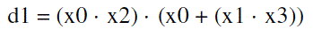
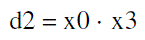
| The proposed LUT-based multiplier for input word-size L = 4 is shown in Fig.3. It consists of a memory-array of eight words of (W +4)-bit width and a 3-to-8 line address decoder, along with a NOR-cell, a barrel-shifter, a 4-to-3 bit encoder to map the 4-bit input operand to 3-bit LUT-address, and a control circuit for generating the control-word (s0 s1) for the barrel-shifter, and the RESET signal for the NOR-cell. The 4-to-3 bit input encoder is shown in Fig.3(b). It receives a four-bit input word (x3 x2 x1 x0) and maps that onto the three-bit address word (d2 d1 d0), according to the logical relations: |
 (1a) (1a) |
 (1b) (1b) |
 (1c) (1c) |
| The pre-computed values of A × (2i + 1) are stored as Pi for i = 0, 1, 2, ·· · , 7 at 8 consecutive locations of the memory array as specified in Table I in bit-inverted form. The decoder takes the 3-bit address from the input encoder, and generates 8 word-select signals, {wi, for 0 ≤ i ≤ 7}, to select the referenced-word from the memory-array. The output of the memory-array is either AX or its sub-multiple in bit-inverted form depending on the value of X. From Table I, we find that the LUT output is required to be shifted through 1 location to left when the input operand X is one of the values {(0 0 1 0), (0 1 1 0), (1 0 1 0), (1 1 1 0)}. Two left-shifts are required if X is either (0 1 0 0) or (1 1 0 0). Only when the input word X = (1 0 0 0), three shifts are required. For all other possible input operands, no shifts are required. Since the maximum number of left-shifts required on the stored-word is three, a two-stage logarithmic barrel The number of shifts required to be performed on the output of the LUT and the control-bits s0 and s1 for different values of X are shown Table I. The control circuit [shown in Fig.3(c)] accordingly generates the control-bits given by |
| s0 = x0 + (x1 + x2) (2a) |
| s1 = (x0 + x1) (2b) |
| A logarithmic barrel-shifter for W = L = 4 is shown in Fig.3(d). It consists of two stages of 2-to-1 line bit-level multiplexors with inverted output, where each of the two stages involves (W + 4) number of 2-input AND-ORINVERT (AOI) gates. The control-bits (s0, ¯ s0) and (s1, ¯ s1) are fed to the AOI gates of stage-1 and stage-2 of the barrel-shifter, respectively. Since each stage of the AOI gates perform inverted multiplexing, after two stages of inverted multiplexing, outputs with desired number of shifts are produced by the barrel-shifter in (the usual) uninverted form. The input X = (0 0 0 0) corresponds to multiplication by X = 0 which results in the product value A · X = 0. Therefore, when the input operand word X = (0 0 0 0), the output of the LUT is required to be reset. The reset function is implemented by a NOR-cell consisting of (W + 4) NOR gates as shown in Fig.3(e) using an active-high RESET. The RESET bit is fed as one of the inputs of all those NOR gates, and the other input lines of (W +4) NOR gates of NOR cell are fed with (W + 4) bits of LUT output in parallel. When X = (0 0 0 0), the control circuit in Fig.3(c), generates an active-high RESET according to the logic expression: |
| RESET = (x0 + x1) · (x2 + x3) (3) |
| When RESET=1, the outputs of all the NOR gates become 0, so that the barrel-shifter is fed with (W + 4) number of zeros. When RESET=0, the outputs of all the NOR gates become the complement of the LUT output-bits. Note that, keeping this in view, the product values are stored in the LUT bit-inverted form. Reset function can be implemented by an array of 2-input AND gates in a straight-forward way, but the implementation of reset by the NOR-cell is preferable since the NOR gates have simpler CMOS implementation compared with the AND gates. Moreover, instead of using a separate NOR-cell, the NOR gates could be integrated with memory array if the LUT is implemented by a ROM [8], [9]. The NOR cells, therefore, could be eliminated by using a ROM of 9 words, where the 9th word is zero and RESET is used as its word-select signal. To compare the area of the proposed LUT-multiplier and the existing LUT-multiplier, we have synthesized the multipliers for L = 4 for different coefficient width W by Synopsys Design Compiler [10] using TSMC 90nm library and listed in Table II. Both the designs have nearly the same data arrival time, but the proposed LUT design is found to offer a saving of nearly 23% of area over the conventional design. The saving in proposed LUT design resulting from lower storage and less decoder complexity is reduced mainly due to the overhead of barrel-shifter and NOR cells (indicated in Table II). Multiplication of an 8-bit input with a W-bit fixed coefficient can be performed through a pair of multiplications using a dual-port memory of 8 words (or two single-port memory units) along with a pair of decoders, encoders, NOR cells and barrel-shifters as shown in Fig.4. The shift-adder performs left shift operation of the output of the barrel-shifter corresponding to more significant half of input by four bit-locations, and adds that to the output of the other barrelshifter. In the next subsection, we present two other optimization schemes which has been proposed recently for reduction of storage size of LUT multipliers [11]. |
V. CONCLUSION
|
| The proposed architecture for multipliers using Look-up table approach for multiplication requires half of the memory compared to the conventional LUT multipliers with same throughput for 4 bit address. The size of LUT is reduced by using Tow-stage logarithmic barrel-shifter and (W+4) number of NOR gates, where W is the word length of fixed multiplying coefficients. The proposed LUT multiplier based design requires half the memory compared to DAbased and conventional LUT based designs at the cost of approximately 4NW AOI gates and nearly 2NW NAND/NOR gates. Therefore FIR filter design based on proposed LUT architecture could be more efficient than DA-based approach in terms of area complexity for a given throughput and lower latency of implementation. Further work is required to find other possibilities of LUT optimization with different address size for better memory utilization. |
Tables at a glance
|
 |
|
| Table 1 |
Table 2 |
|
| |
Figures at a glance
|
 |
 |
 |
 |
| Figure 1 |
Figure 2 |
Figure 3 |
Figure 4 |
|
| |
References
|
- J. G. PROAKIS AND D. G. MANOLAKIS, DIGITAL SIGNAL PROCESSING: PRINCIPLES, ALGORITHMS AND APPLICATIONS. Upper Saddle River, NJ: Prentice-Hall, 1996.
- T. Furuyama, “Trends and challenges of large scale embedded memories,” in Proc. IEEE 2004 Conference on Custom Integrated Circuits, Oct. 2004, pp. 449–456.
- D. G. Elliott, M. Stumm, W. M. Snelgrove, C. Cojocaru, and R. Mckenzie, “Computational RAM: implementing processors in memory,” IEEE Trans. Design & Test of Computers, vol. 16, no. 1, pp. 32–41, Jan. 1999
- “Advanced Approach To Look-up Table Design For Memory Based Realization of FIR Digital Filter” by K.SRIKARSH VARDHAN REDDY International Journal of Scientific & Engineering Research, Volume 3, Issue 9, September-2012 ISSN 2229-5518 IJSER © 2012 http://www.ijser.org
- “New Approach to Look-up-Table Design and Memory-Based Realization of FIR Digital Filter” by Pramod Kumar Meher, Senior Member,IEEE IEEE TRANSACTIONS ON CIRCUITS AND SYSTEMS-I: REGULAR PAPERS 1
- J.-I. Guo, C.-M. Liu, and C.-W. Jen, “The efficient memory-based VLSI array design for DFT and DCT,” IEEE Trans. Circuits and Syst. II:Analog and Digital Signal Process., vol. 39, no. 10, pp. 723–733, Oct. 1992.
- P. K. Meher, “New approach to LUT implementation and accumulation for memory-based multiplication,” in Proc. 2009 IEEE International Symposium on Circuits and Systems, ISCAS ’09, May 2009, pp. 453– 456.
- A. K. Sharma, Advanced Semiconductor Memories : Architectures, Designs, and Applications. IEEE Press, Piscataway, NJ and Wiley-Inter science, Hoboken, NJ, 2003.
- E. John, “Semiconductor memory circuits,” in Digital Design and Fabrication, V. G. Oklobdzija, Ed. New York: CRC Press, 2008.
- “Synopsys, Design Ware. Foundry Libraries, Mountain View, CA.” [Online]. Available: http://www.synopsys.com/
- P. K. Meher, “New look-up-table optimizations for memory-based multiplication,” Submitted to The International Symposium on Integrated Circuits, (ISIC ’09) ’ to be held in December 2009.
|