Research & Reviews: Journal of Material Sciences
ISSN:2321-6212
ISSN:2321-6212
Department of Physics, Faculty of Science, Al-Jouf University, Sakaka, Aljouf, Saudi Arabia
Received date: 17/05/2017; Accepted date: 21/06/2017; Published date: 28/06/2017
DOI: 10.4172/2321-6212.1000174
Visit for more related articles at Research & Reviews: Journal of Material Sciences
The present paper discusses the studies of surface state electrons (SSE) on liquid helium films in confined geometry using suitable substrate structures, microfabricated on a silicon wafer which resembles Field Effect Transistors (so called Helium FET). The sample has a Source and Drain regions, separated by a Gate structure, which consists of 2 gold electrodes with a narrow gap (channel) through which the electron transport takes place. After developing a new model of number of saved electrons as a function of gate barrier, it becomes easier to study the mobility of SSE. The experimental results show a reasonable agreement with the literature.
Micro-structured geometry, Surfacestate electrons, Helium film
The transport of electrons through constrictions has been a topic of considerable interest for decades. Most systems which have been investigated so far were either metal, where point contacts down to the size of a single atom have been realized [1], or semiconductors, e.g. MOSFETs with split gate geometry, where the effective contact size can be tuned electrically by applying a proper gate voltage [2-4]. Surface-state electrons (SSE) above liquid helium form an ideal 2-dimensional electron system (2DES) [5]. The 2-dimensional electron system also exists in semi- conductors and heterostructures. The only measuring techniques which have been applied so far are either the capacitive coupling to this system using the ac techniques [6] or the microwave resonance in a cavity [7]. I have been using samples which resemble MOSFETs, so called He-FETs. The first dc measurements of 2DES on liquid helium with the He-FET have been done during the last 15 years and so far have demonstrated as a proof of principle that the He-FET is functioning [8]. Here the probes are generally in direct contact with the electrons which allows measurements of I-V characteristics. With a central electrode, the gate, this flux can be well controlled. 2-DES on liquid helium has many advantages.
One important advantage is that the electron density can easily be varied continuously from very low values, where the system behaves like a classical gas, to a Wigner crystal, and up to degenerate Fermi-gas because the surface can be charged deliberately from a separate electron source (e.g. tiny heated filament) in very dedicated way. Recent advances in microfabrication technology have allowed the study of SSE in confined geometry using devices such as micro-channel arrays [9-13]. I report here the study of SSE by calculating the mobility of the electrons on He-FET under defined system. A new model of saved electrons as a function of gate barrier [14] has been taken into account to study the mobility of SSE for such system in classical regime. Table 1 show the samples which are used in this work.
Table 1. The four different samples which were used in this paper
| Sample No. | Used Silicon wafer | Shape of the source in front of the gate | Channel dimension | Oxide layer thickness |
|---|---|---|---|---|
| Sample 1 | Non-doped silicon | Triangular | 10 µm × 52 µm | - |
| Sample 2 | Non-doped silicon | Triangular | 10 µm × 2 µm | - |
| Sample 3 | Doped silicon | Triangular | 10 µm × 200 µm | 500 nm |
| Sample 4 | Doped silicon | Rectangular | 10 µm × 100 µm | 500 nm |
The essential parts of the experimental set-up have been described previously [8,15]. A tiny heated filament above the source area supplies the electrons and is operated in a pulsed mode with pulse duration of 25 ms and a repetition rate of 4 Hz to minimize the thermal load. The electrons which have passed through the gate channel to the drain are collected by a pick-up electrode. Whereas in the first experiments with a Helium FET the electrode structures consisted of gold films evaporated on glass, the substrate used in the present work was a piece of a silicon wafer, covered with 500 nm oxide, which formed the sourcechannel- drain area. The split-gate electrodes and also a guard electrode surrounding the whole device consisted of 100 nm gold films evaporated onto the wafer (Figure 1a). A voltage on the order of a few volts was applied to the Si substrate between the source and the drain side. Together with the voltages applied to the split gate and the guard this provides the potential landscape for the electrons on the device (Figure 1b). The sample was positioned at an adjustable height in the gas space above the liquid level of a 4He cryostat and was therefore covered with a super fluid Helium film whose thickness could be controlled between 20 and 60 nm. The temperature in all the measurements was 1.3K.

Figure 1: (a) Si sample (size 22 × 18 mm2) with gold electrodes; (b) potential distributions along the source-gate-drain contour. The channels used in our experiments had a length between 2 and 100 μm and a width of 10 μm.
The idea of pulsing the gate is used to study the electron transport on helium film on confined geometry (He-FET) from source to drain through the gate (the channel) by opening the gate for a very short time (on the order of tens or hundreds nanoseconds) and observe the passed electrons at the pick-up. The number of rest electrons at the source after pulsing the gate is also interesting quantity because, the summation of passed and rest electrons should give the total number of saved electrons for a certain charging time. Figure 2 shows both, the passed and the rest saved electrons at the source (here sample No. 4 was used). The decrease of the rest electrons seems to be an exponential function which can be used to develop a model of relaxation time of the electrons at the source. When we plot the number of rest electrons on a logarithmic scale, we get a more and less linear dependence (Figure 3). Here one could imagine that the source is a capacitor which is charged with a charge Q=Ne, where N is the number of rest electrons at the source, and the channel is a resistor with a constant resistance R.

Figure 2: For sample No. 4: a) the pick-up current (Ip) during pulsing the gate measurement which show the passed and rest electrons. b) The number of passed and rest electrons at the source as a function of pulse width. Here the channel is long (100 μm) and the helium film thickness is ≈50 nm and the average of the initial number of saved electrons before pulsing the gate is 4.0 × 10⁸ electrons.

Figure 3: a) The logarithmic dependence of the number of rest electrons on the pulse width. b) Schematically RC circuit which illustrate the model of the relaxation time on the source.
The simple combination of these two components can be illustrated as an RC circuit as shown in Figure 3b. As we can see from Figure 2b the relaxation time (τ=RC) in this case is in the order of milliseconds. This time constant is a relatively long time compared to the transit time of the electrons through the channel which is in the order of tens of nanoseconds as we will see later. This measurement was repeated using a sample which has a short channel, sample No. 2, and the result as expected has a smaller time scale than the long channel, corresponding to a smaller value of R (Figure 4).

Figure 4: For sample No. 2: The number of passed and rest electrons at the source as a function of pulse width. Here the channel is short (2 μm), the helium film thickness is ≈50 nm and the average of the initial number of saved electrons before pulsing the gate is 7.0 × 10⁸ electrons.
Rest Electrons at the Source after Pulsing the Gate
In general, the number of rest electrons at the source depends on the pulse width and so on the number of pulses and also depend on the driving potential (Us-d). Figure 5a and 5b shows the number of rest electrons at the source as a function of the number of pulses for different pulse widths and different driving potential between source and drain for sample No. 2. As discussed in the previous paper [15], the driving potential depends on the external illumination of light because it increases the conductivity of the silicon wafer. Using sample No. 1 its observed that, the passed electrons increases and so the rest electrons at the source decreases faster with the number of pulses when there is enough external intensity of light (Figure 6). This is because of the generation of electron-hole pairs on the silicon substrate increases when the intensity of light increases.

Figure 5: For sample No. 2: The number of rest electron at the source as a function of pulse width: a) for Vs_d=1.5 V, b) for Vs_d=3.0 V. Here the channel is short (2 μm), the helium film thickness is ≈50 nm and the average of the initial number of saved electrons before pulsing the gate is 4.5 × 10⁷ electrons.

Figure 6: For sample No. 1: The number of rest electrons as a function of number of pulses for different intensity of external light. Here the channel is long (100 μm) and the film thickness is ≈50 nm. One can see that without illumination the transport of the electrons through the channel is much slower, due to the bad conductivity of the substrate, which leads to an ill-defined driving potential.
Passed Electrons, Transit Time, and Mobility Calculation
The transit time is the time needed for the electrons just to pass through the channel. We measured the transit time as the following:
a) Setting the electrode potentials and switching on the filament and see the dc pick-up current.
b) Setting the gate voltage such as we observe a maximum current at the pick-up and registering this value because we will use it to open the gate later.
c) Switching off the filament to start with empty source.
d) Close the gate completely by applying a certain negative potential (-3 V at the normal condition) to the gate and switching on the filament again.
e) Charge the source for a certain charging time and switching off the filament.
f) Open the gate for a very short time by pulsing the gate using squired pulse with a certain pulse width and observing the past electrons at the pick-up.
g) Repeat these steps for different pulse widths starting from 10 ns and observe at which transit time the first small peak at the pick-up occurs.
h) Open the gate completely and see the number of rest electrons at the source.
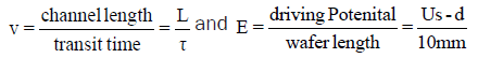
Using sample No. 1 with 1 V driving potential (Us-d=1 V), Figure 7 shows the increasing of passed electron (represented on the peaks observed at the pick-up) as a function of pulse width. As we can see the first peak in this case appear at 100 ns, so the time needed to cross at least half of the channel is 100 ns1 and so the transit time then would be τ=200 ns in this case. The mobility can be calculated from the following equation:

Figure 7: For sample No. 1: a) the pick-up current as a function of time for different pulse widths for a long channel sample. b) The total passed electrons calculated from the area under pick-up current graph for each pulse width. Here the channel is long (100 μm) and the film thickness is ≈50 nm and Vs-d=1 V.
ν=μ.E (1)
Where ν, μ, and E are the speed of the electrons, mobility of the electrons, and the electric field respectively. The speed of the electrons and the electric field can be determined from:
For sample No. 1:
Us-d=1 V, τ=200 ns, L=100 μm, and so the mobility μ=5 × 104 cm2/Vs.
For sample No. 2:
Us-d=2 V, τ=20 ns, L=2 μm, and so the mobility μ=0.5 × 104 cm2/Vs.
For sample No. 3:
Us-d=2 V, τ=1000 ns, L=200 μm, and so the mobility μ=2.0 × 104 cm2/Vs.
As we can see from the data and calculations, the transit time depends on the channel length. The average value of the mobility is ≈2.5 × 104 cm2/Vs. The mobility values calculated from these results are one order of magnitude less than the mobility of the SSE on bulk helium at the same temperature which is in the order of 1 × 105 cm2/Vs. In general the mobility of the electrons on films is relatively low compared to that on bulk helium at the same temperature because of the stability of the electrons on films is less and the roughness of the substrate reduces the velocity and so the mobility the SSE. Furthermore, it is also shown that the transit time depends on the He-film thickness and the roughness of the substrate. This will be a very interested topic for the next paper.
The results presented here demonstrate that SSE in confined geometry are well suited for investigating the transport of correlated electrons in the classical (Coulomb regime), which is not directly accessible with electrons in solid state systems. The mobility values of SSE on helium films which have been determined seems to have reasonable values compare to the values determined at the same conditions on bulk helium.
I thank Professor P Leiderer and E Scheer for useful discussions and Louis Kukk for technical help. Gratefully acknowledges support by DAAD.