INTRODUCTION
|
| The IRTS roadmap predicts that the 90% of SoC is covered with memory by the year 2K13. Because of the high speed, low power consumption, robustness and ability of integrating with digital logic blocks.so the bigger the size of SRAM larger is the power consumed. We many reasons for using SRAM in system design. Speed, cost, density and features are the main design tradeoffs for selecting SRAM for your design. When speed is considered SRAM has an edge over DRAM. |
| Due to this many attempts were being made to decrease the power consumption in SRAM which will increase the battery lifetime of the devices which were operated using battery such as PDA’s, wireless, cellular phone and low power biomedical devices. For this scaling of supply voltage is an effective method. But due to this the gate delay is increased which reduces the frequency of operations. |
| This concept charge sharing is used in architectural level, but we are implementing at the cell level of design on the single ended SRAM’s. |
EXISTNG WORKS
|
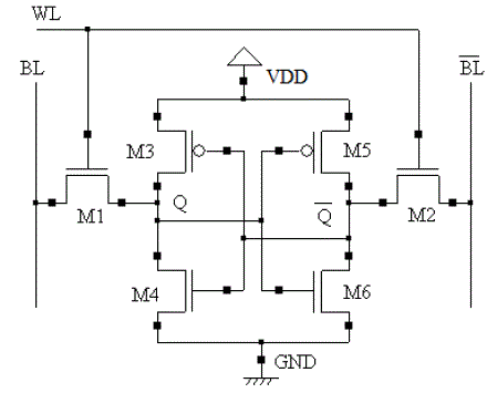
| 1. Conventional 6T SRAM design: There are many topologies for SRAM in past decades 6T SRAM got its attention for the tolerance capability for noise over another SRAM cell design. The 6T SRAM cell design consists of two access transistors and two cross coupled CMOS inverters. Bit lines are the input/output ports of the cell with high capacitive loading. The operations READ and WRITE are conducted by these bit lines only, we will see how these are carried out. |
| ïÃâ÷ Read Operation: Before starting of the read operation, we should charge the bit lines to VDD. When the word line (WL) is enabled, the bit line which connected to the node of the cell containing ‘0’ is discharged through the NMOS transistor. |
| By this we can know which node is containing’0’ and which is having ‘1’ in it. Using sense amplifiers we can know the node containing 1/0 by sensing the bit lines. The bit line containing ‘1’ means it's connected to the node containing ‘1’ and vice versa. |
| ïÃâ÷ Write Operation: For writing 1/0 we should provide the data to the bit line (BL), with respect to the bit line bar (BL). When the word line (WL) is enabled the data is written into respective node. |
| But the conventional 6T SRAM have stability limitations at low supply voltages. Hence we go for 8T SRAM design. It has the advantage of low power at read ’1’operation. As it does not consume power at read ‘1’ cycle. |
| 2. Single-ended 8T SRAM cell:In the 8T RSAM, we have the normal 6T SRAM with the read decoupled path consisting of two NMOS transistors. Let us see how read and write operation are carried out. |
| ïÃâ÷ Read operation: First we should pre-charge the bit lines to full swing after the pre-charge phase is completed we should assert the read word line (RWL) which drives the access transistor M5 ON. The transistor (M6) is ON if the data at node Q is ‘0’, due to which read bit line is grounded through transistors M5 &M6.when the RBL is sensed we have the value in the node ‘0’. Like this way can do read operation also during which we will have value in RBL as ‘1’ indicating read ‘1’ value due to not having an discharge path . |
| ïÃâ÷ Write operation: The write operation is same as in the 6T SRAM except the write replaces the precharge circuit. |
| 3. 10T SRAM (charge sharing): In 10T SRAM is similar to the 8T SRAM with extra transistors are connected to the read decoupled path with bit lines (BL &ïÿýïÿýïÿýïÿýïÿýïÿýïÿýïÿýïÿýïÿýïÿýïÿý) to avoid the draining of read current to ground. |
| ïÃâ÷ Read operation: Here for read operations are carried depending on the last written data.The last written data is ‘0’ then BLB is high and BL is low, the value read was ‘0’ then the read bit line (RBL) discharges M5,M6 and M7 to BL . |
| ïÃâ÷ Write operation: If In next cycle we want to write ‘1’then BL is to be driven from mid-level voltage to full swing as BL is already at mid-level voltage. Likewise we can use the read discharge power for the reduction of write power. |
| If in next cycle we want towrite’0’ then BL is grounded. As bit lines are at some mid-level voltages they are to be grounded. |
PROPOSED SRAM DESIGN
|
| Here the proposed SRAM design is using the concept of charge sharing from the above 10T SRAM design. But the difference is that the design is done with less number of transistors when compared to the above 10T SRAM which also decreases the area of the design And in the proposed design we also reduced the power consumption when compared with the previous designs. |
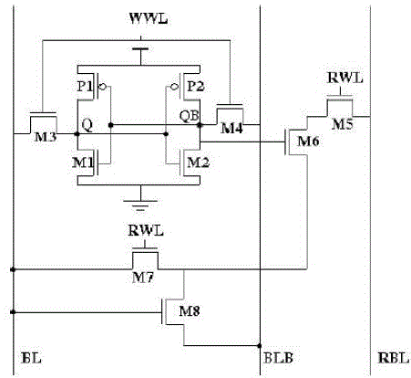
| The proposed SRAM consists of a single ended 7T bit cell which has one bit line (BL) for write operation and one Read Bit cell for read operation. |
| During the write operation WWL was enabled and RWL was disabled (i.e RWL=’0’) so M4 M5 M6 are in the off state. The cell acts like single ended 5T SRAM Cell and writes the Bit line data into the cross coupled inverter pair P1 M3 and P2 M2. |
| During the read operation the bit line disconnected from inverter pair because of WWL=’0’ during read phase and RWL was enabled so M6 M5 will be in the ON state. For read operation here we are using separate bit line called RBL instead of using same BL. SO during read operation RBL was pre-recharged. |
| Read ‘0’: In reading ‘0’ M4 was ON state, so RBL has a discharging path from M4 M5 and M6, the M6 will acts like a charge sharing network, instead of discharging the charge to the ground M6 will charge the bit line (BL) so there will no loss of power to the ground. |
| Read’1’: In reading ‘1’ M4 was OFF state so there will be no discharging path for RBL to discharge maintains the charge and reads the ‘1’ |
SIMULATON AND RESULTS
|
| These SRAM designs are designed and simulated using S-edit and T-Spice using TSMC018 technology in Tanner Tools 13.0. The Conventional 8T SRAM, 10T SRAM and Proposed SRAM are simulated with different voltages and there power dissipations are compared and shown in below tables. |
CONCLUSIONS
|
| Here we have seen a novel approach for designing SRAM for dynamic power reduction. We have used the previous designs of SRAM of charge sharing and designed a design with minimum area and power as well. The proposed design will reduce the both write power and read power. |
Tables at a glance
|
|
|
| |
Figures at a glance
|
 |
 |
 |
| Figure 1 |
Figure 2 |
Figure 3 |
|
| |
References
|
- Kevin, Z., Embedded Memories for Nano-Scale VLSIs. 2009: Springer Publishing Company, Incorporated. 400.
- Brown, A.R., Roy, G., and Asenov, A., Poly-Si-Gate- Related Variability in DecananometerMOSFETs With Conventional Architecture. ElectronDevices, IEEE Transactions on, 2007. 54(11): p. 3056-3063.
- Bo, Z., et al. A Sub-200mV 6T SRAM in 0.13um CMOS.inSolid-State Circuits Conference, 2007. ISSCC 2007. Digest of Technical Papers. IEEEInternational. 2007.
- Cheng, B., Roy, S., Roy, G., Brown, A., and Asenov, A. Impact of Random Dopant Fluctuation on Bulk CMOS 6-T SRAM Scaling. inSolid-StateDevice Research Conference, 2006. ESSDERC 2006.Proceeding of the 36th European. 2006.
- Jawar Singh, D.K.P., Simon Hollis, and Saraju P. Mohanty, A single ended 6T SRAM cell design for ultra-low-voltage applications.IEICEElectronicsExpress, 2008.5(18): p. 750-755.
- Mizuno, H. and T. Nagano, Driving source-line cell architecture for sub-1-V high-speed low-power applications. Solid-State Circuits, IEEE Journal of,1996.31(4): p. 552-557.
- Takeda, K., et al., A read-static-noise-margin-free SRAM cell for low-VDD and high-speed applications. Solid-State Circuits, IEEE Journal of,2006.41(1): p. 113-121.
- Chang, L., et al., An 8T-SRAM for VariabilityTolerance and Low-Voltage Operation in High-Performance Caches.Solid-State Circuits, IEEEJournalof, 2008.43(4): p. 956-963.
- Tae-Hyoung, K., et al. A High-Density Subthreshold SRAM with Data-Independent Bitline Leakage and Virtual Ground Replica Scheme.inSolid-StateCircuits Conference, 2007. ISSCC 2007. Digest of Technical Papers. IEEE International. 2007.
- Wang, X., Roy, S., and Asenov, A., Impact of Strain on the Performance of high-k/metal replacement gate MOSFETs, in Proc. 10th UltimateIntegration on Silicon (ULIS 2009). 2009.
|