This paper demonstrates a CMOS frequency synthesizer design, whose primary purpose is to test the designer’s high speed, mixed-signal CMOS circuit design skill. Line codes are the techniques for representing digital sequences by pulse waveforms suitable for baseband transmission. NRZ or non return to zero is an important Line coding method. NRZ pulses are of full bit duration. We do not get square waveform in conventional current starved VCO. So, the conventional current starved VCO cannot be used for generating NRZ line coding as it is necessary that the output waveform of VCO should be square wave for NRZ coding. This new current starved CMOS VCO is used to design a DPLL. Furthermore, this DPLL design is used to generate a clock for a 8.33Mbits/second with NRZ data format for center frequency at VCO. The DPLL presented here uses XOR phase detector for reducing jitter noise and divide by two stage is used in the feedback loop for frequency synthesis. The DPLL is designed uses active PI filter.
Keywords |
| DPLL, VCO, Active PI Filter, jitter noise. |
INTRODUCTION |
| The digital phase –locked loop, DPLL, is a circuit that is used frequently in modern integrated circuit design. |
| Consider the waveform and block diagram of a communication system is shown in figure.1. Digital data is loaded into
the shift register at the transmitting end. The data is shifted out sequentially to the transmitter output driver. At the
receiving end, where the data may be analog after passing through the communication channel, the receiver amplifies
and changes the data back into digital logic levels[1]. The DPLL performs the function of generating a clock signal
which is locked or in synchronization with the incoming signal. The generated clock signal is used in the receiver to
clock the shift register and thus recover the data. This application of a DPLL is often termed a clock recovery circuit or
bit synchronization[2,3].This paper aims at “VLSI implementation of DPLL frequency synthesizer for NRZ-line
coding” .In this paper, a XOR DPLL is designed using active Proportional Integral filter which has center frequency 8.33 MHz, lock time 8.8μs and 1MHz lock in range. The significance of this DPLL is to generate a clock for a 8.33
Mbits/s data stream with data format non–return to zero level or simply NRZ level. This is the major advantage of
using NRZ code; that is, the data rate can be twice the channel bandwidth.The objective is to design a DPLL for a
signal whose output frequency is 8.33 MHz and has a lock range of 1 MHz. This PLL is designed for being used in
some specific circuit design, for e.g. Carrier-Recovery, Data synchronization, demodulator, and so on. |
DESIGN SPECIFICATION OF DPLL |
| Design specification of DPLL is shown in Table 1 |
TEST SPECIFICATION |
| Test specification of DPLL is shown in table 2 |
DESIGN OF XOR DPLL USING ACTIVE FILTER |
| For designing XOR DPLL using active PI filter, we have used a current starved VCO cascaded with Schmitt trigger
this generates square waveform which is used as the input for frequency divider circuit which consist of D flip flop and
the output of this frequency divider goes in the loop filter. Next we select the loop filter values in order to keep the
DPLL from oscillating. Design of XOR DPLL using active filter is shown in fig. 2 |
A. Design of Active Loop Filter |
| The clock misalignment encountered in a DPLL XOR PD and passive filter using an XOR PD and passive filter can
be minimized by using the active proportional integral(active PI) loop filter shown in fig 3. |
| Transfer function of this filter is given by: |
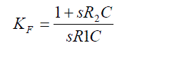 |
| The natural frequency of the resulting second-order system is given by |
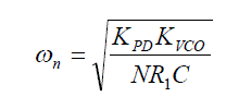 |
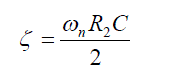
| And the damping ratio is given by : |
 |
| The lock range is given by |
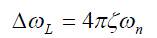 |
| The pull in range, using the active PI loop filter, is limited by the VCO oscillating frequency. |
Calculation of R1, R2 and C of active filter: |
| The gain of the VCO is |
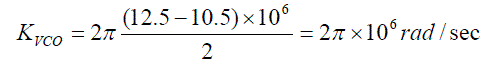 |
| The gain of phase detector is |
| KPD =5/π |
| Now, we calculate the natural frequency using equation.. and assuming ζ=0.7 , |
| ΔfL =1 MHz so |
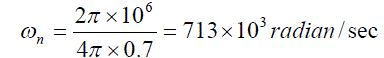 |
| Using equations 2 and 3 with N=2, we can solve them for R1C and R2C as approximately 9.835μs and
1.9635μs.respectively. |
 |
| Now the designed DPLL has the following specifications : |
| The VCO has center frequency 8.33MHz |
| The lock range between DATA and DCLOCK is set to ΔfL =1 MHz |
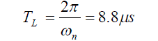
| The lock time TL=8.8 μs[4,5]. |
| B. Simulation Result of XOR DPLL Using Active Filter |
| Simulation of XOR DPLL using active filter is shown in fig 4 [6,8]. It can be seen from the simulation results shown in
figure 4 that the desired results are achieved. The first waveform represents VCOIN, this is the input voltage of VCO,
the middle one represents DCLOCK, this is the input voltage of XOR PD and the last waveform represents CLOCK,
which is the input of active filter. A square wave as required by NRZ coding is received and the lock range of the
DPLL is increased to 1 MHz. This means that the loop will lock up on an input frequency from 3.17 MHz to 5.17 MHz
and generate an output frequency two times the input frequency in lock time TL=8.8μs. In the fig 4, the width of one bit
data is 120 ns(=1/8.33 MHz).The frequency of the DPLL output clock is 8.33 MHz. |
| divide by two stage is used in the feedback loop to make dclock=4.17 MHz. If the data input is an alternating series
of ones and zeros then the frequency of the resulting square wave is 4.17 MHz,or one–half of the data rate.
This is the major advantage of using NRZ code; that is ,the data rate can be twice the channel bandwidth[7,8] . |
CONCLUSION |
| Based upon this study and simulation, these components are selected for DPLL which is used for NRZ line
coding.CMOS VCOs are designed using Schmitt trigger. Primarily there are two methods to design VCO.One uses ring
oscillator and other uses Schmitt trigger. In recent years, ring oscillators have become an essential building block in
VCO’s[4]. They can provide a wide operating range, a small layout area and ease of integration. In this paper, VCOs
are designed using current starved VCO and schmitt trigger and then transient analysis is carried out to observe the
NRZ waveform of each VCO.Here DPLL is designed using XOR PD which has good noise rejection. XOR DPLL
having current starved CMOS VCO using Schmitt trigger which has center frequency of 8.33 MHz .This CMOS VCO
has direct relationship between voltage and frequency and is linear in frequency range 5.7MHz-12.5MHz. Active PI
loop filter is used in XOR DPLL for reducing the clock misalignment which encountered in a DPLL. In this paper, We
have designed a XOR DPLL using active PI filter which have center frequency 8.33 MHz ,lock time 8.8μs and 1MHz
lock in range. Finally,The significance of this DPLL is to generate a clock for a 8.33 Mbits/s data stream with data
format non –return to zero level or simply NRZ level.The width of one bit data is 120 ns(=1/8.33 MHz).The frequency
of the DPLL output clock is 8.33 MHz.A divide by two stage is used in the feedback loop to make dclock=4.17 MHz.
If the data input is an alternating series of ones and zeros then the frequency of the resulting square wave is 4.17
MHz,or one–half of the data rate This is the major advantage of using NRZ code ;that is,the data rate can be twice the
channel bandwidth . |
Tables at a glance |
 |
|
| Table 1 |
Table 2 |
|
Figures at a glance |
 |
 |
 |
 |
| Figure 1 |
Figure 2 |
Figure 3 |
Figure 4 |
|
References |
- R. E. Best, Phase-Locked Loops: Design, Simulation, and Applications. New York: McGraw-Hill, third ed.,1997.
- B. Razavi, “A study of Phase Noise in CMOS Oscillators”, IEEE J. Solid-State Circuits, vol.31,pp.331343,1996.
- B. Razavi, “Monolithic phase locked loops and clock recovery circuits theory and design”,IEEE Press,pp.283377and381483,1996.
- B.Keeth, R.J.Baker, and H.W.Li “CMOS Transconductor VCO with adjustable operating and center frequencies,” Electronics Lettes,Vol.31
- F. M. Gardner, Phaselock Techniques. New York, NY: John Wiley & Sons, second ed., 1979. ISBN 0-471-04294-3.
- Tanner EDA User Guide
- J. Maneatis, “Low-jitter process-independent DLL and PLL based on self-biased techniques,” in ISSCC 1996 Dig. Tech. Papers, Feb. 1996.
- R.Jacob Baker , Harry W.Li , David E.Boyce, CMOS- Circuit ,layout and Simulation, PHI ,1998.
|