Keywords
|
| LECC (logical error correction circuit), LLECC (Low logic error correction circuit), HLECC (High logic error correction circuit) |
I. INTRODUCTION
|
| With the growing demand of handheld devices like cellular phones, multimedia devices, personal note books etc., low power consumption has become major design consideration for VLSI circuits and system. With increase in power consumption, reliability problem also rises and cost of packaging goes high. Power consumption in VLSI circuit consists of dynamic and static power consumption. [5] Dynamic power has two components i.e. switching power due to the charging and discharging of the load capacitance and the short circuit power due to the non-zero rise and fall time of the input waveforms. The static power of CMOS circuits is determined by the leakage current through each transistor. Power consumption of VLSI circuits can be reduced by scaling supply voltage and capacitance. With the reduction in supply voltage, problems of small voltage swing, insufficient noise margin and leakage currents originate. With the development of technology towards submicron region leakage power has become significant component of total power dissipation. Static power component of power consumption must be given due consideration if current trends of scaling of size and supply voltage need to be sustained.[5] |
| In System on chip (SoC) design, different parts like digital, analog, passive component are fabricated on a single chip and needs different voltages to achieve optimum performance.[2] Level converters are used to convert the logic signal from one voltage level to other level and are the significant circuit component in VLSI systems. Level shifters are also important circuit component in multi voltage systems and have been used in between core circuits and I/O circuit. |
| One approach has been to increase the drive current of the level shifter by enlarging the transistor channel width. Another is to use a multi-stage level shifters [5] or inverters with multiple supply voltages. However, these circuits still depend on the supply voltage difference, the circuit configuration is complex, and it requires multiple references voltage. The problem discussed above is thus basically unresolved. |
| To solve this problem, we presented the logical error correction circuit (LECC) capable of handling extremely low voltage input. The proposed LS circuit can convert extremely low voltage input signal into high voltage output signal. In this paper, we will first examine the performance of conventional level shifter circuit without LECC and with LECC at very low voltage into high voltage. |
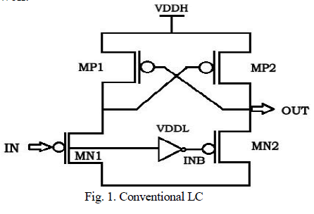
II. CONVENTIONAL LS CIRCUIT
|
| Fig .1 The cross couple PMOS transistors improve the switching speed and output swing by using the positive feedback. [1] When a „1âÃâ¬ÃŸ is applied to IN, INB becomes „0âÃâ¬ÃŸ and OUT is pulled down which turn on MP2 and OUT goes to VDDH. When IN changes to „0âÃâ¬ÃŸ, INB rise to VDDL and turns on MN2 which pulls OUT down to 0. However, if subthreshold logic signal is used for the input to the level converter, due to the low voltage value of logic „1âÃâ¬ÃŸ at INB, the on current through MN2 is very weak comparing with the on current of MP2. Node OUT cannot be pulled down and the conventional LC will not functional well. |
 |
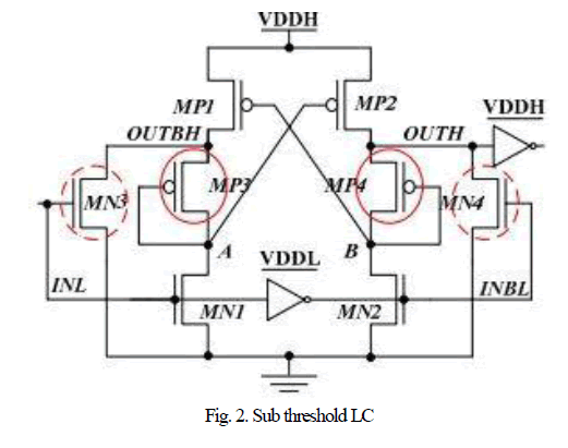
III. SUB-THRESHOLD LS CIRCUIT
|
| The sub-threshold level converter we additional PMOS diode (MP3 and MP4) are connected in series with the 2 original cross-coupled PMOS transistors (MP1 and MP2).[3] When the LC is steady state, the |VGS| of the PMOS diode is very small which equals to the diode voltage drop |VPD|. At the same, the original pull-up PMOS transistors are either turned on of turn off, depending on the input value. For the cross-couple LC design, the input voltage should be able to activate the LC internal positive feedback in order to make the LC flip its output correctly. [6] When the sub-threshold logic „1âÃâ¬ÃŸ is inputted to the NMOS gate. In power aware systems, supply voltage is varied to match with the weak load of the system. Therefore the circuit performance has to be adaptive with the operating supply voltage. Fig.2. |
 |
IV. LECC APPROACH
|
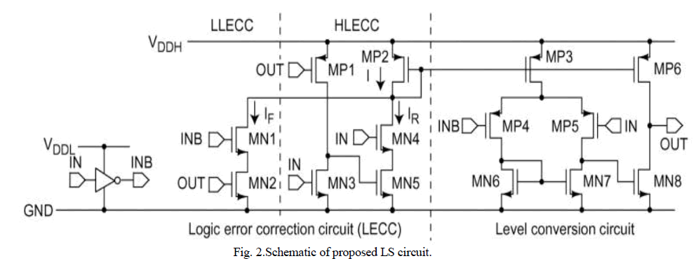
| It consists of a level conversion circuit and a logic error correction circuit (LECC). The complementary input signals (IN and INB) and the output signal (OUT) are applied to the LECC. The LECC supplies the operating current for the level conversion circuit only when the LECC detects a logic error. Fig. 3 shows the complete schematic of the LS circuit. The operation principles of the circuits are described in the following sections. |
| 1) Level Conversion Circuit: The level conversion circuit, which is shown on the right in Fig. 3, is based on a conventional two-stage comparator circuit. The comparator generates output voltage signal, OUT, according to the difference in the voltage of IN and INB. Note that the voltage of OUT is determined by the drive currents of pull-up transistor MP6 and pull-down transistor MN8, and that the currents flowing in MP6 and MN8 depend on current flowing through MP2. Therefore, because both drive currents are determined by the same current, the circuit is free from the limitations discussed in the conventional ones. |
| In the conventional comparator design, a current reference circuit needs to operate steadily. However, because the current circuit needs to operate steadily. However, because the current reference circuit dissipates static current and increases power dissipation, it cannot be used in our design. Therefore, we developed a logic error correction circuit (LECC) in which the current flowing in the circuit is generated only when the input signal change. |
| 2) Logic Error Correction Circuit (LECC):[4] The LECC, is shown on the left in Fig. 3, consists of two circuit blocks: 1) a low logic error correction circuit (LLECC) and 2) a high logic error correction circuit (HLECC). They are driven by IN, INB, and OUT. The LECC generates an operating current such that IN and OUT correspond to each other. When the output logic level of the LS circuit corresponds to the input logic level, the LECC does not supply current . When they do not correspond, the LECC detects the logic error, and the LLECC or HLECC supplies an operating current. In other words, because the LECC supplies an operating current only when the input and output logic levels do not correspond to each other, the power dissipation of the circuit is minimized. The correction circuit operations are described below. |
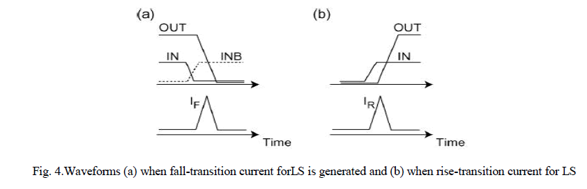
| LLECC: The low logic error correction circuit, LLECC, Consists of two nMOSFETs (MN1 and MN2) connected in series. The LLECC operates only when OUT does not correspond to the "Low" logic of IN. Fig. 4 depicts the waveforms of IN, INB, and OUT. When IN changes from High to Low, or when INB changes from Low to High, there is a period during which OUT does not correspond to IN. During this period, the LLECC generates fall-transition current ___until OUT corresponds to the Low logic of IN |
| HLECC: The high logic error correction circuit, HLECC, consists of three nMOSFETs (MN3, MN4 and MN5) and a pMOSFETs (MP1). In contrast to the LLECC, the circuit operates only when OUT does not correspond to the "High" logic of IN. Fig. 4 depicts the waveforms of IN and OUT. When IN changes from Low to High, there is a period during which OUT does not correspond to IN. During this period, the HLECC generates rise-transition current until OUT corresponds to the High logic of IN. |
| When IN and OUT are High and Low, the output voltage of the first stage are is High because the overdrive voltage of the MP1 is larger than that of MN3. This enables MN4 and MN5 to supply current to the level conversion circuit, and pulls OUT up to VDDH. From the discussion above, current for the level conversion circuit is expressed as |
| I = IF + IR |
| Because IFand IRare not generated and the LECC does not supply current when the input and output logic levels which correspond,[7]&[8] the power dissipation of the circuit is minimized. The amount of IFand IR generated depends on lower supply voltage of VDDL. |
| When IN and OUT correspond, the LECC does not supply any current to the level conversion circuit. However, in fact, leakage current flows in the circuit.[9] Therefore, because the voltage gain in the level conversion circuit is sufficient to keep the output node, OUT is kept at a voltage, i.e. VDDH or GND |
 |
IV. SIMULATION RESULT
|
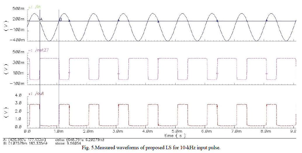
| The performance of the proposed LS circuit evaluated using CADENCE with a set of GPDK 180 and GPDK 90 . VDDHwas set to 3v[]. We used an inverter as a load circuit of the LS circuit and calculated power dissipation include a charge and discharge current of the load. [11]The amplitude and frequency fINof the input signal were set to 0.4v and 1Khz input signal was converted into a 3-v output signal fig .4. |
 |
 |
V.CONCLUSION
|
| Here we presented a level shifter circuit for extremely low-voltage. The proposed circuit consists of a conversional level shifter circuit and sub threshold level converter.[10] It can convert low-voltage digital input signals into highvoltage digital output signals and achieve low power operation. I am using CADENCE GPDK 180 AND GPDK 90 CMOS technology file and demonstrated its operation by measurements. The circuit converted a 0.4-V input signal into a 3.-V output signal. |
ACKNOWLEDGMENT
|
| I sincerely acknowledge in all earnestness, the patronage provided by our Director Dr. C.Muthamizhselvan, Engineering & Technology, to endeavour this project.I wish to express my deep sense of gratitude and sincere thanks to our Professor and Head of the Department Dr. S. Malarvizhi, for her encouragement, timely help and advice offered to me.My sincere thanks to our project coordinatorDr. M. Malathi, Professor, Electronics and Communication Department, for his encouragement and advice.I am very grateful to my guide Mr J. Selvakumar, Assistant Professor (Sr.G) who has guided with inspiring dedication, untiring efforts and tremendous enthusiasm in making this project successful and presentable. |
| I extend my gratitude and heart full thanks to all the staff and non-teaching staff of Electronics and Communication Department and to my parents and friends, who extended their kind co-operation by means of valuable suggestions and timely help during the course of this project work. |
References
|
- Wang and A. Chandrakasan,” A 180 mV FFT processor using sub-threshold circuit techniques.” in IEEE ISSCC Dig. Tech. Paper, 2004, pp.292-293.
- S. Henzler, “Power Management of digital circuit in Deep Sub-Micron CMOS Technologies”. New York: Springer, 2007.
- Huishao and chi- Ying Tsui, “A Robust, input voltage adaptive and low energy consumption level converter for sub- threshold logic”, in IEEE,2007.
- Yuji Osaki, Tetsuya Hirose, “A Low Power Level Shifter with logic error correction for extremely low voltage digital CMOS LSIs”, in IEEEJOURNAL of SSC, vol.47, No.7
- P. Chandrakasanet.al., (1995) “Minimizing power consumption in digital CMOS circuits,” Proceedings of the IEEE, vol.83, no.4, pp.498-523.
- S. Lütkemeier and U. Rückert, “A subthreshold to above-threshold level shifter comprising a wilson current mirror,” IEEE Trans. Circuits Syst.II, Exp. Briefs, pp. 721–724, 2010.
- Liu, Kramer, Indiveri, Delbruck and Douglas,“Analog VLSI : Circuit and priciples”, The MIT press.
- Paul R.Gray, Paul J. Hurst, Stephen h. lewis,“Analysis and design of analog integrated circuit, fourth edition”, John wiley& sons, INC.
- Bob Dobkin and Jim wiliams,“Analog circuit design”, LINEAR technology.
- www.researchgate.net ,technology help.
- Manoj Kumar, SandeepK.Arya and SujataPandey,” Level shifter design for low power application”, IJCSIT VOL.2, NO. 5, October 2010.
- www.cadence.com, software help.
|