Keywords
|
| Bandpass filter, electromagnetic bandgap (EBG), ultra wideband (UWB), wideband filter. |
I.INTRODUCTION
|
| The Ultra-wideband (UWB) technology is being reinvented recently with many promising modern applications. In particular, the UWB radio system has been receiving great attention from both academy and industry since the Federal Communications Commission (FCC) release of the frequency band from 3.1 to 10.6 GHz for commercial communication on applications in February 2002[1]. In an UWB system, an UWB band pass filter (BPF) is one of the key passive components to keep the spectrum of the signals to meet the FCC limits, or used in the UWB pulse generation and reshaping. |
| In such a system, an UWB filter is one of the key components, which should exhibit a wide bandwidth with low insertion loss over the whole band. In order to meet the FCC limit, good selectivity at both lower and higher frequency ends and flat group-delay response over the whole band are required .Over the last years, thedesign of wide and ultra-wide Bandpass filters is generating a great interest due to the fast development of broadband wireless communication systems. Traditional methods to implement ultra-wide bandpass filters usually introduce spurious bands .These undesired bands become an important drawback for ultra-wide bandpass filters performance due to their proximity to the pass-band of interest. |
| The recent research and development practical applications of EBG structures have improved realizing compact EBG structures filters. EBG structure recently is developed rapidly due to its unique properties to suppress the propagation of surface wave in microstrip filters. EBG structure is also known as a high impedance surface due to its ability to suppress the propagation of surface wave at the certain operational frequency. This structure is also has ability to block the effect of mutual coupling effect in array application. |
II.OVERVIEW OF EBG STRUCTURES
|
| 2 EBG definition. |
| Periodic structures are abundant in nature, which have fascinated artists and scientists alike. When they interact with electromagnetic waves, exciting phenomena appear and amazing features result. In particular, characteristics such as frequency stop bands, passbands, and band gaps could be identified. |
| Electromagnetic band gap structures are defined as artificial periodic (or sometimes non-periodic) objects that prevent/assist the propagation of electromagnetic waves in a specified band of frequency for all incident angles and all polarization states. |
| Electromagnetic band-gap (EBG) structures are periodic structures which can prohibit the propagation of electromagnetic wave in certain band of frequency. They can be embedded in the dielectric substrate or etched on the metal layers. The EBG structures are always used to help suppress the surface waves to gain good pass band or stop band. |
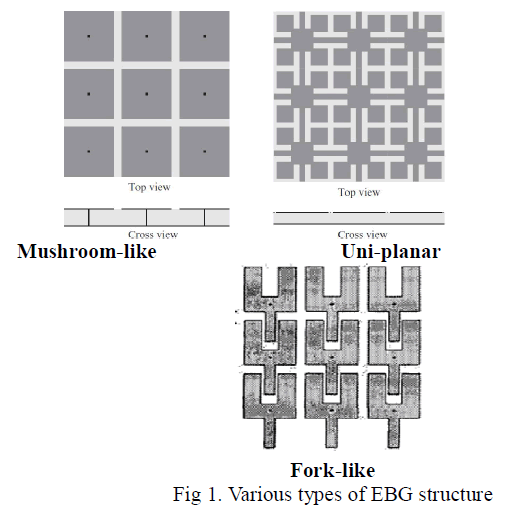
| There are two types of EBG structure to be discussed. Firstly is Perforated dielectric and the second one is Metallodielectric structures. Perforated dielectric is defined as effectively suppress unwanted substrate mode. This structure designed by drill periodic holes on dielectric subtracts to introduce another dielectric but in practical, this structure is difficult to implement. Metallodielectric structure is exhibits an attractive reflection phase future where the reflected field change continuously from 180 degrees to -180 degrees versus frequency. |
III.ELECTROMAGNETIC BAND GAP (EBG) STRUCTURE
|
| EBG structures are usually realized by periodic arrangement of dielectric materials and metallic conductors. In general, they can be categorized into three groups according to their geometric configuration: |
| (1) Three-dimensional volumetric structures, |
| (2) Two-dimensional planar surfaces, and |
| (3) One-dimensional transmission lines. |
 |
IV.BASIC PRINCIPLE OF EBG STRUCTURE
|
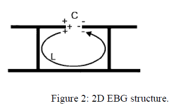
| The basic design of EBG structure is shown in figure 2. known as mushroom like EBG structure. This structure has frequency range where the surface impedance is very high. The equivalent LC circuit acts as a two-dimensional electric filter in this range of frequency to block the flow of the surface waves. The central frequency of the band gap is shown in equation 2. The inductor L results from the current flowing through the visa, and the capacitor C due to the gap effect between the adjacent patches. Thus, the approach to increase the inductance or capacitance will naturally result in the decrease of band-gap position. |
 |
IV.FILTER THEORY
|
| In designing a filter, the following important parameters are generally considered. |
| • Pass bandwidth |
| • Stop band attenuation and frequencies |
| • Input and output impedances |
| • Return loss |
| • Insertion loss |
| • Group delay |
| The most important parameters among the above is the amplitude response given in terms of the insertion loss Vs frequency characteristics. Let Pi be the incident power at the filter input , Pr is the reflected power, PL is the power passed on to the load. The insertion loss of the filter is defined by, |
| IL (dB) =10log (Pi/PL) = -10 log(1-|ÃÂÃâ|2) |
| Where PL=Pi - Pr, if the filter is lossless |
| and ÃÂÃâ is the voltage |
| reflection coefficient given by |ÃÂÃâ|2 = Pr/Pi |
| The return loss of the filter is defined by |
| RL (dB) =10log (Pi/Pr) = -10log|ÃÂÃâ|2) |
| which quantifies the amount of impedance matching at the input port. |
| The group delay is important for the multi-frequency or pulsed signals to determine the frequency dispersion or deviation from constant group delay over a given frequency band and is defined by |
| Td= [1/2π]*[dÃÂät/df] |
| Where ÃÂät is the transmission phase. |
V.PROPOSED EBG STRUCTURE.
|
| The conventional EBG structure has a wide band-gap and compact nature. The inductor L results from the current flowing through the connecting via. The gap between the conductor edges of two adjacent cells introduces equivalent capacitance C. Thus a two dimensional periodic LC network is realized which results in the frequency band-gap and the center frequency of the band-gap is determined by the formula |
| ω = 1/√LC |
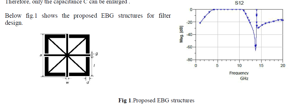
| From above equation it can be seen that in order to achieve an even more compact EBG structure, the equivalent capacitance C and inductance L should be increased. But in the EBG design procedure, if the dielectric material and its thickness have been chosen, the inductance L cannot be altered. Therefore, only the capacitance C can be enlarged . |
 |
VI.DESIGN OF PROPOSED UWB FILTERS
|
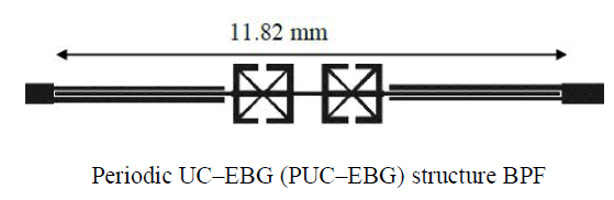
| In this proposed model two uwb band pass filter are designed and simulated also compared with performance of EBG Embedded Multi Mode Resonator BPF. All BPFs are fabricated with thickness of 0.635 mm on an RT/Duroid substrate with a dielectric constant of10.2 . The schematics of uniplanar compact–EBG (UC–EBG) structure and a periodic UC–EBG (PUC–EBG) structure are shown in fig 2. The inter digital coupled lines used in all BPFs have a coupling peak at the center frequency of 6.85 GHz. Simple EBG Embedded Multi Mode Resonator UWB BPF is also shown in fig 2. There simulation as been done using ADS Momentum simulator |
 |
VI.SIMULATION RESULTS
|
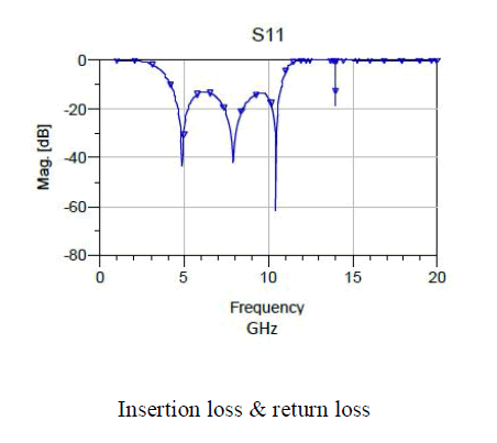 |
VII.CONCLUSION
|
| In this, EBG structures are investigated and applied to UWB BPFs. The UC–EBG cell ,used here as improved passband obtained in UWB region,also improving the good out-of-band performances and the EBG structure to reduce the overall size of the filter. There results have been compared by simulated using ADS Momentum simulator. |
References
|
- FCC, Revision of Part 15 of the Commission’s Rules Regarding Ultra-Wideband Transmission Systems FederalCommunications Commission, Tech. Rep. ET-Docket 98-153, FCC02-48, Apr. 2002.
- H. Ishida and K. Araki, “Design and analysis of UWB bandpass filter,” in Proc. IEEE Top. Conf. Wireless Comm.Tech., Oct. 2003, pp.457–458.
- C.-L. Hsu, F.-C. Hsu, and J.-T. Kuo, “Microstripbandpass filters for ultra-wideband (UWB) wireless communications,”inIEEE MTT-S Int.Dig., Jun. 2005, pp. 679–682.
- W. Menzel, M. S. R. Tito, and L. Zhu, “Low-loss ultra-wideband (UWB) filters using suspended stripline,” in Proc.Asia-Pacific Microw.Conf., Dec. 2005, vol. 4, pp. 2148–2151.
- K. Li, D. Kurita, and T. Matsui, “An ultra-wideband bandpass filter using broadside-coupled microstrip-coplanarwaveguide structure,” in IEEE MTT-S Int. Dig., Jun. 2005, pp. 675–678.
- J.-S. Hong and H. Shaman, “An optimum ultra-wideband microstrip filter,” Microw. Opt. Technol. Lett., vol. 47, no. 3,pp. 230–233, Nov.2005.
- L. Zhu, S. Sun, and W. Menzel, “Ultra-wideband (UWB) bandpassfiltersusing multiple-mode resonator,” IEEE Microw. Wireless Compon.Lett., vol. 15, no. 11, pp. 796–798, Nov. 2005.
- F.-R. Yang, K.-P. Ma, Y. Qian, and T. Itoh, “A uniplanar compact photonic-bandgap (UC-PBG) structure and itsapplications for microwave circuit,” IEEE Trans. Microw. Theory Tech., vol. 47, no. 8,pp. 1509–1514, Aug. 1999.
- Microstrip Filters for RF/Microwave Applications JIA-SHENG HONG,M. J. LANCASTER ,JOHN WILEY & SONS,INC 29
- Application of Electromagnetic Bandgaps to the Design of Ultra-Wide Bandpass Filters With Good Out-of-BandPerformance. IEEE TRANSACTIONS ON MICROWAVE THEORY AND TECHNIQUES, DECEMBER 2006
- Recent Development of Ultra-Wideband (UWB) Filters IEEE 2007 International Symposium on Microwave, Antenna,Propagation, and EMC Technologies.
- Electromagnetic Band Gap Structures in Antenna Engineering . FAN YANG,YAHYA RAHMAT-SAMII
|