International Journal of Advanced Research in Electrical, Electronics and Instrumentation Engineering
ISSN ONLINE(2278-8875) PRINT (2320-3765)
ISSN ONLINE(2278-8875) PRINT (2320-3765)
Joffie Jacob1, Reshmi V2
|
| Related article at Pubmed, Scholar Google |
Visit for more related articles at International Journal of Advanced Research in Electrical, Electronics and Instrumentation Engineering
With the increased use of sophisticated electronic equipments, high efficiency variable speed drives and power electronic controllers power quality has become a rising concern to both utilities and customers. Voltage sag is the most common power quality problem generally caused by faults in transmission/distribution sector. Voltage sag even lasting only for a few tens of milliseconds is enough to bring entire production lines to standstill causing considerable economic loss. Therefore necessary measures have to be taken to protect sensitive loads which are susceptible to these voltage disturbances. Among the available solutions, Dynamic Voltage Restorer (DVR) is a series connected cost effective custom power device that can quickly mitigate the voltage sag in the system and restore the load voltage to the pre-fault value. Traditional DVR consists of series and shunt converters connected back-to-back and a dc capacitor installed on the common dc link. But the cost, weight, and physical size have inhibited the DVR from greater penetration and wider recognition. In this paper, two no energy (source side and load side connected shunt converter) system topologies for dynamic voltage restorers are analysed based on the storage element required for sag mitigation. In the former case the dc capacitor is required to store the necessary energy for compensation but in the latter case it is required only for smoothing the dc-link voltage so that size of the energy storage element required can be reduced significantly. A synchronous reference frame based controller for the inverter based voltage sag compensator is presented. This paper also deals with a method to mitigate the zero-sequence voltage component in the load after the occurrence of an unbalance voltage sag. Simulations are carried out in PSCAD software package.
Keywords |
| Power quality, voltage sag, custom power device, dynamic voltage restorer, dc capacitor |
I. INTRODUCTION |
| In recent years both utilities and customers have reported a rising tide of misadventures related to power quality. The industries like process industries, petrochemical industries and semiconductor industries use equipments which are very sensitive to voltage distortions [1]. These critical processes have costly consequences if disturbed by poor power quality. Voltage sag is a frequent voltage disturbance in the power system. 92% of the interruptions in industrial installations are due to voltage sag. For these reasons there is a growing interest in equipments for the mitigation of these disturbances. Custom Power (CP) devices employ power electronic controllers for the purpose of supplying a level of power quality that is needed by customers [3]. DVR is a series connected compensating device that protects sensitive load from voltage disturbances. This is performed by rapid series voltage injection to compensate for the drop in the supply voltage. |
| DVR is a device gaining popularity due to the increase sensitivity of industry to voltage sag. However the need for reduction in cost, weight, and physical size has inhibited the DVR from greater penetration and wider acceptance [7]. A traditional DVR consists of back to back connected series and shunt converter and a common dc capacitor. The DVR injects three-phase compensating voltages in series to the power line The energy required for the compensation of voltage sag is taken from the dc capacitor or other energy-storage elements. In this paper, source side and load side connected shunt converter (no-energy storage) system topologies for dynamic voltage restorers are analysed.Most of the DVR design the restoration of positive-sequence and compensation of negative sequence are taken into consideration, while zero-sequence components are ignored. But the low voltage distribution systems in a lot of countries are made up of three-phase four-wire system. Therefore the zero-sequence components will necessarily appear due to unbalance of three phase voltages. A disadvantage of the zero-sequence components is higher insulation costs, asymmetry of the phases and magnitudes of the terminal voltages [8]. A method for the mitigation of zerosequence voltage component in the load after the occurrence of unbalance voltage sag is also presented. |
| This paper is organized as follows: Section I gives an Introduction regarding the need of custom power device for the elimination of power quality problems affecting the sensitive load. Section II is helpful to understand the causes and effects of voltage sag. Section III explains about Dynamic Voltage Restorer. Section IV illustrates the Synchronous reference controller. Section V explains the need for zero sequence voltage control. Section V compares the performance of the two Dynamic Voltage Restorer topologies based on the energy storage element requirement and the last section VI concludes the paper followed by the references. |
II. VOLTAGE SAG |
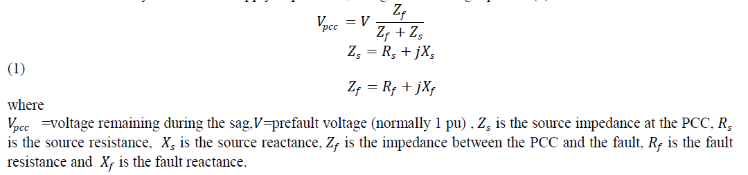
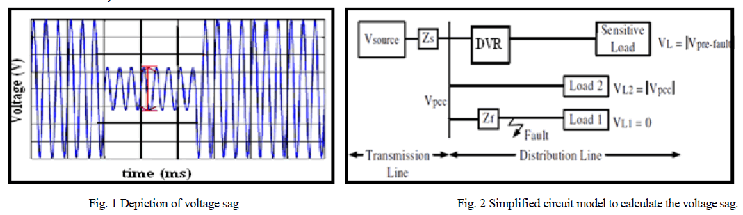
| Voltage sag is defined as a short duration reduction in the rms supply voltage that can last from 0.5 cycles to 1 sec, with typical dip depth ranging from 0.9 to 0.1 pu of a 1-pu nominal voltage [4]. Voltage sag is caused by faults (more than 70% are weather related such as lightning) on the transmission or distribution system or by switching of loads with large amounts of initial starting or inrush current such as motors, transformers and large dc power supply [2]. Fig. 1 shows the voltage sag waveform caused by a remote fault condition. Voltage sag is usually caused by a short circuit current flowing into a fault and a simplified model is illustrated in Fig. 2. Magnitude and phase of the voltage sag at the PCC are determined by the fault and supply impedances, using the following equation (1) |
 |
 |
III. DYNAMIC VOLTAGE RESTORER |
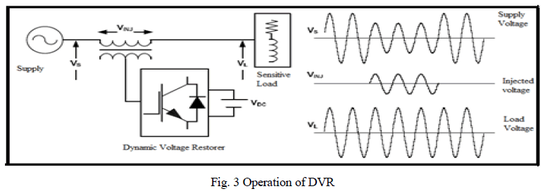
| In order to overcome the power quality problems the concept of custom power devices is introduced recently. One of those device is the Dynamic Voltage Restorer (DVR), which is the most efficient and effective device used in power distribution networks. DVR is a series connected solid state device as shown in Fig. 3 that injects voltage into the system in order to regulate the load side voltage. It is normally installed in a distribution system between the supply and the critical load feeder at the PCC. |
 |
| A. Power Circuit Topologies of DVR |
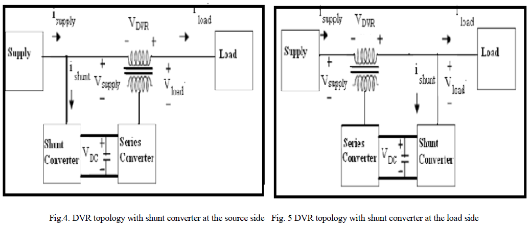
| During a voltage dip the DVR injects voltages and thereby restores the supply voltages. In this phase the DVR exchanges active and reactive power with the surrounding system. If active power is supplied to the load by the DVR it needs a source for the energy. In the no-storage DVR concept, the DVR has practically no energy storage and the energy is taken from the remaining supply voltage during the voltage dip. It has a disadvantage of an increase in the supply current. The advantages are cost saving of the energy storage and the ability to compensate long duration voltage dips. Topologies for DVR using power from the grid (no-storage )can generally be characterized with the location of the shunt converter e.g. at the supply side of the series converter or at the load side of the series converter. Topologies with power from the supply can be [6] , |
| 1) Source side connected passive converter: In Fig. 4 when a voltage drop appears at the source side or at the ac terminals of the shunt converter it loses its rectification capability when the maximal source voltage gets lower than the dc-link voltage. Therefore, the series converter requires a large dc capacitor as an energy-storage element intended for feeding electric dc power to the series converter [7]. |
| 2) Load side connected passive converter: No voltage drop appears at the load side or at the ac terminals of the shunt converter in Fig. 5, because the series converter compensates for voltage sags. In this case, the electric power required for voltage-sag compensation comes from the shunt converter to the series converter. In other words, the dc capacitor does not play any role in feeding the electric power required for compensation to the series converter. Thus, the DVR can continue operating properly, independent of the long or short duration of voltage sags [7]. |
 |
IV. SYNCHRONOUS REFERENCE FRAME CONTROL SCHEME |
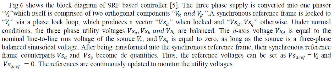 |
| If voltage sag occurs, the latest update of the references will be locked and used to calculate the compensation voltage. The core of this controller is the phase-locked loop (PLL) which locks the synchronous reference frame to the positive-sequence component of the supply. Once voltage sag is detected, the sampling process will be locked and the existing values in the sample and hold will be used as voltage references for compensation. Whenever faults occur, the resulting voltage sags translate into the reduction of positive-sequence component. The sag compensator inverter will be started if the positive sequence magnitude ïÿýïÿýïÿýïÿýïÿýïÿýïÿýïÿý dropped below a preset threshold level ïÿýïÿýïÿýïÿýâÃâÃŽ . |
 |
V. ZERO SEQUENCE VOLTAGE CONTROL METHOD |
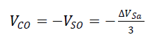
| Most faults in power systems are single-phase faults. Therefore the zero-sequence components are occurred during faults. This section deals with a control method that can mitigate the zero-sequence under the unbalance faults causing voltage sag. Fig.7 shows the phasor diagram of the source and compensating voltages when this control method is applied to the DVR.A voltage-sag depth in each phase is given as a voltage reference to each single-phase converter |
| When voltage sag occurs in the a-phase, the three-phase compensating voltages are given by the following |
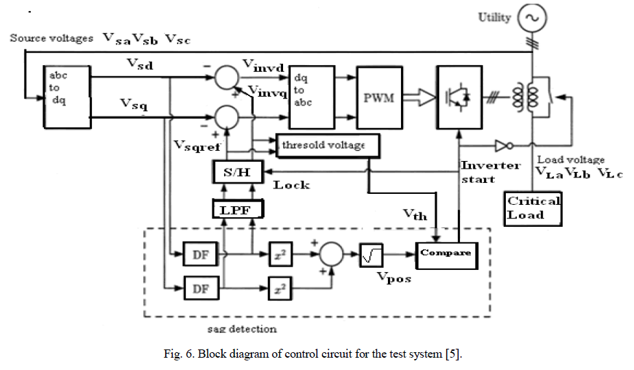
| This single-phase voltage sag may produce a zero-sequence voltage in the source. Thus, the DVR should inhibit the zero sequence voltage from being applied to the load in a three-phase four-wire system. The zero-sequence component in the compensation voltages vco is represented by the following: |
 (4) (4) |
| As a result, Vco cancels out the zero-sequence voltage and no zero-sequence voltage appears in the load voltage |
 |
VI. SIMULATION CIRCUITS AND RESULTS |
| This section discusses about the simulation models and results obtained. Both the source side and load side shunt converter topology are taken into consideration. Simulations are done in PSCAD .Table 1 gives the circuit parameters. |
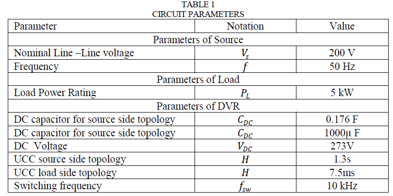 |
| A. Simulation Circuit of source side connected shunt converter DVR topology |
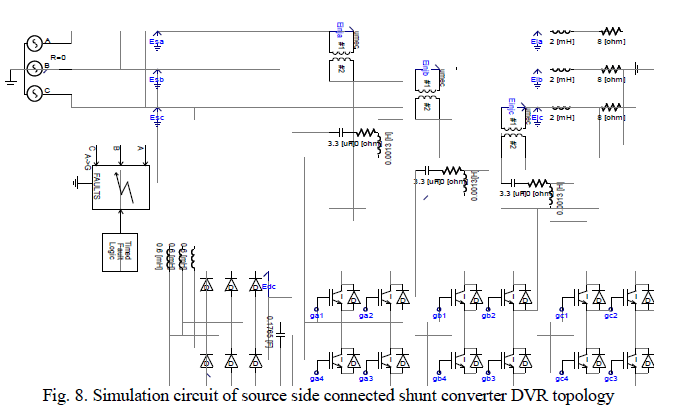 |
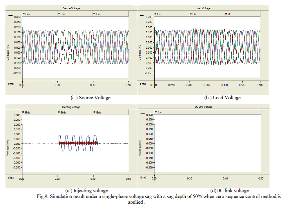
| 1) Single Phase voltage sag: Fig. 9 illustrates the source voltage, load voltage, injecting voltage and dc link voltage when the control method of zero-sequence voltage is applied to series converter. |
 |
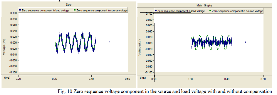
| 2) Zero sequence voltage comparison: Fig.10 illustrates the zero sequence component in the source and load voltage with and without compensation |
 |
| B. Simulation Circuit of load side connected shunt converter DVR topology |
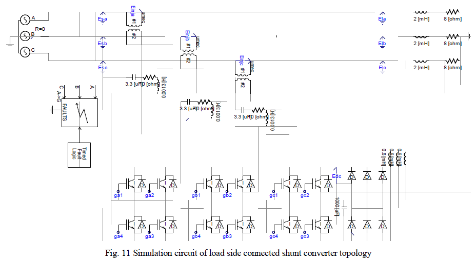 |
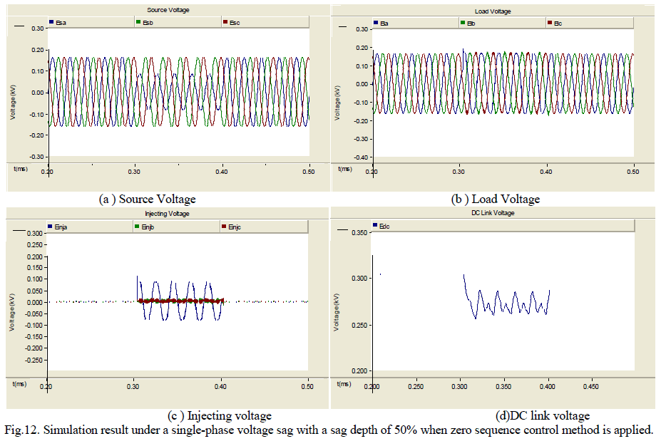
| 1) Single Phase voltage sag: Fig illustrates the source voltage, load voltage, injecting voltage and dc link voltage when the control method of zero-sequence voltage is applied to series converter. |
 |
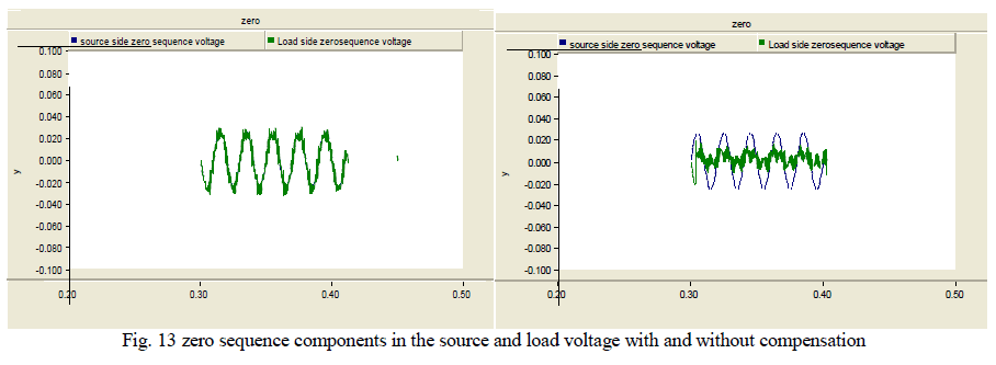
| 2) Zero sequence voltage comparison: Fig.13 illustrates the zero sequence components in the source and load voltage with and without compensation |
 |
VII. CONCLUSION |
| The simulation results clearly shows that by connecting the shunt converter to the load side the required dc link capacitor value can be reduced. The source side shunt converter requires a capacitance value of 0.176 F, while the load side shunt converter topology requires only 1000μF for the mitigation of voltage sag with 50% sag depth. The zero sequence compensation discussed will eliminate undesired zero sequence voltage component which is coming in the load after the occurrence of an unsymmetrical voltage sag. |
References |
|