Index Terms
|
| CNTFET, 3VL, HSPICE, Multi threshold value. |
I. INTRODUCTION
|
| A one-bit memory cell is a basic building block of designing array of memory structure and for huge storage memory devices. There are two operations are to be performed in memory cell, they are read operation and write operation. The read operation is to obtain a data value from the cell, write operation is to store a data in to the memory cell. One-bit memory cell can be either latch or flip flop. This memory cell can be for designing SRAM, DRAM, PROM, Mass storage like hard disk, flash memory, memory cards etc. They can be even used in microprocessors and in microcontrollers as ROM array and RAM cells of required size. The access time to the memory cell must be faster and should consume less power. |
| Traditionally, memory cell was designed with binary logic using MOSFET with CMOS technology. The miniaturization of electronic components has been a great deal towards the VLSI industries which give rise to many advanced FETs and efficient logic design. The key features of these advancements in FETs are designing low power, high speed digital circuits. The advanced FETs are FinFET, CNTFET, QDGFET, SET etc and efficient logics are reversible logic, multi-value logic, and adiabatic logic. The memory cell is designed with CNTFET using ternary logic, which is part of multivalue logic. Ternary logic is also known as 3-value logic. |
| The carbon nanotube field-effect transistor (CNTFET) is a rising technology to a well known bulk MOSFET for low-power and high-performance designs due to the realistic transport [4]–[6]. In a CNTFET, the threshold voltage is determined by chirality factor and hence the diameter, so a multi-threshold design can be consummated by using CNTs with different diameters in a CNTFET. The design of a 3value logic family using CNTFETs has been contemplated in [7]; the basic 3 value gates have been presented. 3value arithmetic circuits such as a full adder and multiplier have been contemplated as examples of the application of a 3value gate technique. Simulation results have confirmed [7] that significant power and delay advancements are possible by utilizing this 3 value logic family at both gate and circuit levels. It is said that a design methodology using the CNTFET- based 3 value logic is a feasible solution for low power and high performance VLSI circuit design in the submicron nano ranges[7]. |
| Our goal is to design promising memory cell with CNTFET using 3 value logic which can perform both read and write operation with low power consumption and high switching speed. Large amount of data can be stored in minimum chip area. A carbon nano-tube (CNT) is a excavated cylinder comprises of one or more layers of graphene atoms arranged in a hexagonal network structure. A CNT with many layers is called as multiwall CNT and a CNT with simple singular layer of carbon atoms is called a single-wall CNT. A single-wall CNT can act as either a metal or a semiconductor; build upon on the angle of the atomic arrangement along the CNT. Multi-wall CNT mostly exhibits conducting behavior because of the increased clusters carbon atoms around them having a conducting shell. Many using semiconducting SWCNTs to design electron devices contradictory to MOSFETs; these devices are known as CNTFETs, also called TUBEFETs. CNTFETs are promising nanoscale devices for designing highperformance circuits. There are vast application where high speed, low powered RAM, ROM required in fabricating integrated circuits like multi-core processors, microcontrollers and other digital ICs. This Memory can be used as the module in SoC architecture |
| The ternary cell utilizes the chirality feature of CNTFETs for threshold voltage control, such that there is no need to provide additional power supply levels for ternary operation. The separate features of the proposed circuit for the write and read operations make this design very efficient. |
| The rest of this paper is organized as follows. Section II starts with a carbon nanotube transistors, followed by the review of 3 value logic in Section III. A 3 value logic memory cell is then proposed, analyzed, and evaluated with respect to the write and read operations in Section IV. Traditional performance measures for a memory cell design, such as area, power and delay are simulated by HSPICE in Section V, with conclusion in Section VI. |
II. CARBON NANOTUBE FIELD-EFFECT TRANSISTOR
|
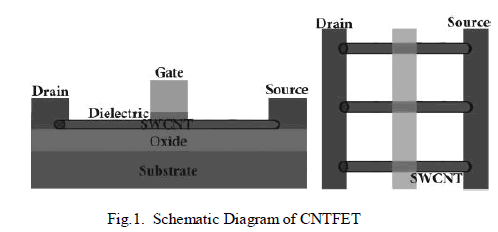
| Carbon Nano-Tube Field Effect Transistor(CNTFET) is one of the advanced FET technology in the VLSI industry. The remarkable electrical properties of carbon nano-tubes arise from the unified electronic network structure of graphene itself that can binded up and form a excavated cylinder. The CNT is connected between source and drain regions acts as the channel material as in the MOSFET device. The diameter of such carbon nano-tube can be expressed in terms of a chirality vector, which connects two crystallo-graphically equivalent sites of the two-dimensional graphene sheet. Here n and m are integers representing the hexagonal lattice. This structure can be described by an index with a pair of integers (n,m) that define its chirality vector. An SWCNT can act as either a conductor or a semiconductor, depending on the dimemsion of the atomic alignment along the tube. In terms of the integers (n,m), the nanotube diameter Dt |
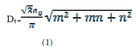 |
| where a0 = 0.142 nm is the inter-molecular distance between each carbon atom and another adjacent atom. Fig. 1 shows the schematic diagram of a CNTFET [9]– [11]. Similar to a conventional MOSFET device, we have four terminals in CNTFET. As shown in Fig. 1, lightly doped semiconducting nano tubes are placed under the gate region which is insulator when unbiased, and heavily doped CNT segments are placed at the either end of the drain and source side to allow for a low series resistance in the ON-state [4]. As the gate potential increases, the device is electro statically turned ON or OFF, with the help of gate. |
| In the last decade two different CNTFET circuit design techniques have been used in the literature, One of them is directly replacing the MOSFET with CNTFET to approach better performance; The second is used CNTFET as a particular nanotechnology devices with its powerful CNT characteristics [8]. Fig.1 shows the schematic diagram of CNTFET. Transistors which use SWCNT have many benefits rather than silicon MOSFET counterpart such as high density of on current and moderately high Ion/Ioff ratio that has many effects on transistors behavior, molecular size, high theoretical transition frequency and changeable threshold voltage depending on carbon nanotube diameter which is an important characteristic of CNTFETs. |
 |
| The threshold voltage is defined as the required voltage required to turn ON the transistor; the threshold voltage of the intrinsic CNT channel can be approximated to the first order as the half-band gap that is an inverse function of the diameter [9]–[11]: |
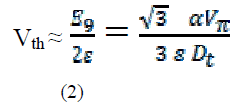 |
| where a = 2.49 A° is the carbon to carbon atom distance, Vπ 3.03 eV is the carbon π–π bond energy in the tight bondingmodel, e is the unit electron charge, and Dt is the CNT diameter. |
| As the diameter of CNT changes, the threshold voltage of the CNTFET will also change. Assume that m in the chirality vector is always zero; then, the ratio of the threshold voltages of two CNTFETs with different chirality vectors is given as |
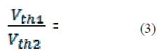 |
| Equation (3) shows that the threshold voltage of a CNTFET is inversely proportional to the diameter of the CNTs.For example, the threshold voltage of a CNTFET using (13, 0) CNTs is 0.428 V, compared to a (19, 0) CNTFET with a threshold voltage of 0.293 V. CNTFETs provide a ideal characteristics to control the threshold voltage by changing the diameter of the CNT [8]. [18], [19] have reported advances in fabrication processes for welldefined CNTs. It is demonstrated in [20] that a postprocessing technique to adjust the threshold voltage of multiple-tube CNTFETs. In this paper, a multi-tube CNTFET-based design is utilized when designing the ternary memory cell. The techniques for changing threshold voltage in multi tube CNTFET is similar to above process all the CNTs will have same diameter. |
III. THREE VALUE LOGIC DESIGN
|
| A three-value logic system was first developed by Jan Lukasiewicz, in 1920, in its popular paper O Logice Tr´ojwarkoscioewj, [12], as abstraction of the traditional binary logic. Three-value logic system has better characteristic compared to previous binary system such as increased bit handling capability per unit area, reduced number and complexity of interconnections, as well as reduced number of active FETs inside a chip. Hence, in the circuit which designs base on three-valued logic, circuits will be simpler and more flexible also more easy. By using 3VL higher speed and less power dissipation will be achieved [13] [14]. To obtain 3value logic system we need three values, in conventional binary system we have two logics values ‘0’ and ‘1’, these logics represented by 0V and Vdd respectively. By supplementing one state between these two logics of conventional binary system ternary logic system can be achieved. In 3value logic system values represented by 0V, Vdd/2 and Vdd which denote ‘0’, ‘1’ and ‘2’ respectively. |
| In principle, 3VL can provide a means of increasing data processing capability per unit chip area. The serial and serial-parallel arithmetic functions can be carried out faster if the 3value logic is employed. One of the main merit of 3value logic is that it reduces the number of required computation steps. As each input can have three distinct values, the number of digits required in a 3VL family is log32 times less than that required in binary logic. It is assumed that 3value logic elements can operate at a speed approaching that of the corresponding binary-logic elements. However, if the 3VL and binary logic gates are used to take advantage of their respective merits, performance could be significantly improved because 3value logic gates are good candidate for decoding block since it requires less number of gates while binary logic gates are a good candidate for fast computation modules. Thus, 3value design technique combined with the conventional binary logic gate design technique also provides an excellent speed and power consumption characteristics in memory circuits. |
| Expanding the present logic levels to 3value logic and higher levels, higher processing rates could be achieved in various applications like memory management, communication throughput and domain specific computation. An evident merit of a 3value logic representation over binary is economy of digits. In binary system, one needs 59% more digits than that of 3value logic system. |
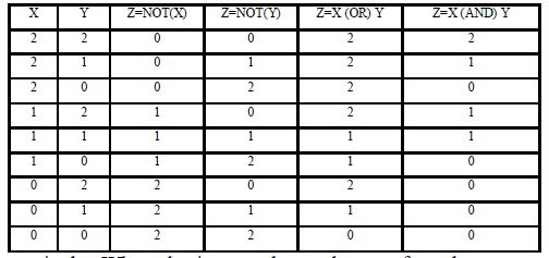
| Three value logic functions are defined as the functions having convincing if a third value is introduced in to the binary logic. Here, 2, 1, and 0 denote the 3 logic values to represent true, intermediate, and false, respectively. Any n-variable {Z1 ,. . .,Zn} 3 value logic function f(Z) is defined as a logic function mapping {0,1,2}n to {0,1,2}, where Z = {Z1 ,. . .,Zn}. The basic operations of 3value logic can be defined as follows, where Zi,Zj {0,1,2} |
| Zi | Zj = max{Zi,Zj} |
| Zi & Zj = min{Zi,Zj} |
| Zi = 2− Zi |
| where “−” denotes the arithmetic subtraction, the operations “|,” “ &,” and “−” are referred to as the OR, AND, and NOT in 3value logic, respectively. The 3 value logic gates are designed according to the convention defined in above equation. Here work the set {0, 1, 2} is used, where 0 = false, 1= intermediate, and 2 = true. Table 1 shows the truth table of all the basic 3Value logic gates. The choice of these values leads in a more natural way the adaptation of the ideas from the binary logic. |
| TABLE 1 TRUTH TABLE FOR 3VALUE LOGIC GATES |
| A. 3VL Standard Inverter design |
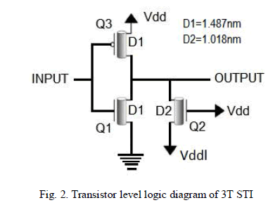
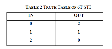
| Ternary inverters are in three different types: standard ternary inverter (STI), negative ternary inverter (NTI) and the positive ternary inverter (PTI). The NTI and the PTI are contorted binary inverters and do not have an output value of logic {1}. The truth-table for the three types of STI is shown in Table 2. The STI is the basic building block for the proposed memory cell design because of its ability to produce logic {1} at the output. Here we consider two different design of the STI the first design is based on the work in [27]. A complementary CNTFET network can also be used for ternary logic design to achieve good performance, low power consumption. |
| The 3T STI consist of three CNTFETs out of which there are two N-CNTFETs namely Q1,Q2 and one PCNTFET Q3. The chiralities of the CNTs used in Q1, Q2, and Q3 are (19, 0), (19, 0), and (13, 0), respectively. From (1), the diameters of Q1, Q2, and Q3 are 1.487, 1.487, and 1.018 nm, respectively. Therefore, the threshold voltages of Q1, Q2, and Q3 are 0.289V, 0.559V, and 0.428V [26]. Here we need to provide two power supplies Vdd and Vddl. This particular design is used in area constrained applications as transistors are just three in number. Power consumption is high in this type of STI is not advisable for digital circuit design. |
 |
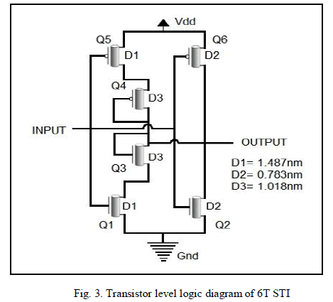
| The 6T STI consists of six CNTFETs, in which there are three N-CNTFET Q1, Q2, Q3 and three PCNTFFET Q4, Q5, Q6 The chiralities of the CNTs used in (Q1,Q5) and (Q2,Q6) and (Q3,Q4) are (19, 0), (10, 0), and (13, 0), respectively. Their diameters of Q1, Q2, and Q3 are 1.487, 0.783, and 1.018 nm, respectively. Hence, the threshold voltages of Q1, Q2, and Q3 are 0.289, 0.559, and 0.428 V, respectively. The threshold voltages of Q5, Q6, and Q4 are −0.289, −0.559, and −0.428 V, |
 |
| respectively. When the input voltage changes from low to high at the power supply voltage of 1V, At the start, the input voltage is lower than 300 mV. This makes both Q5 and Q6 turn ON, both Q1 and Q2 turn OFF, and the output voltage 1V, which is logic 2. As the input voltage increases beyond 300mV, T6 is OFF and T5 is still ON. Where, Q1 is ON and Q2 is OFF. |
| Once the input voltage exceeds 0.6 V, both Q5 and Q6 are OFF, and Q2 is ON to pull the output voltage down to zero. The input voltage transition from high to intermediate and then to low transition is similar to the low to intermediate then to high transition. This 6T- STI is used in most of the digital design based on the logic used. Other logic gates like NOR, NAND gates can be designed using this ternary logic. The main requirement of ternary logic is multi-threshold voltage FET devices. In case of MOSFET, multi-threshold voltage can be obtained using multiple power supplies which causes size and cost of a simple inverter is very much higher than of other type of FETs. But in the CNTFET multi-threshold voltage can be obtained by changing diameter of the carbon nano-tube which is used in the corresponding STI. FET, with single power supply can be used for all the CNTFETs used in the circuit. Table 2. Shows the truth table of 6T |
 |
 |
IV. 3VL MEMORY CELL DESIGN
|
| The memory cell is used to store one bit in it for the some time period until next write operation is performed. The read operation will not affect the value stored in the circuit. The memory cell is the basic storage unit in all semiconductor memories like RAM, ROM, Flash memories. The simple memory was constructed with back to back inverters are used in traditional memory cells as basic components of the storage element for the correct states; access transistors (such as pass or transmission gates) are commonly used to read and write from the back to back inverters. The design requirement for a memory cell is usually specified as follows: when the cell is holding the data (i.e., the access transistors are OFF), the cross coupled inverters must be able to hold the bi-stable states; when the cell is ready to write or read (i.e., the access transistors are ON), then the access transistors must be able to update the correct state from the word lines, or pass the current state to the word lines. The traditional CMOS cell in a binary memory system uses six transistors (6T); two NMOS access transistors and two back to back CMOS inverters. The STI shown in Fig. 2 can be used as a basic storage element of the ternary memory cell. For the read and write operations, single-ended read and write access mechanisms are used. There must be a delay between read and write operation to avoid error of misread in the circuit. |
| A. Block Diagram |
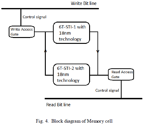
| The basic block diagram of the memory cell which is designed is shown in the Fig. 4. The standard 3VL inverter which is used here is shown in 2 consist of 6- transistors. The read operation and write operation is carried out separately with the help of access gates. These access gates is comprised of transmission gate or pass transistor logic. The read access gates consist of a buffer with the control gate. Buffer is a two transistor inverter designed using CNTFET. The CNTFET used in the circuit has 18nm channel width |
| The write line is connected to the STI-1 when the transmission gate present the corresponding node is ON and the data in the write line is latched in the inverter circuits until the next write operation. Similarly the output of the cross coupled inverters is connected to read bit line when corresponding transmission gate is ON. The simple inverter used here provides the needed delay. This delay must be greater than that of the write delay in order to avoid the misreading error. |
 |
| B. Circuit Diagram |
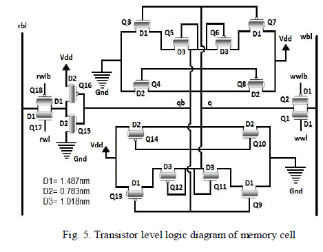
| The proposed ternary memory cell design is shown in the schematic form in Fig. 4 The write bit line wbl, is connected to the input of the write access gate which is a transmission gate. The transmission gate consist of two control inputs write word line bar, wwlb and write word line wwl. When wwl is High the transmission gate is ON and the wbl is connected to the input q of the cross coupled inverters. What ever logic value present in the wbl is sent to the memory cell. The read bit line rbl, is connected to the input of the write access gate which is a transmission gate. When rwl is high the transmission gate is ON and the rbl is connected to the input q of the cross coupled inverters. What ever logic value present in the memory cell is sent to the rbl with a delay due to the buffer. The operation of the proposed memory cell can be described as when the memory cell is holding logic “1”, transistors Q3, Q5, Q6, Q7, Q9, Q11, Q12, Q13 are ON to hold both nodes q and qb to the value of 1/2 Vdd; and when the memory cell is holding logic “0”, transistors Q6,Q7, Q8, Q9, Q10, Q11 are on to hold node q to 0 and node qb to the value of Vdd; When the memory cell is holding logic “2”, transistors Q3,Q4, Q5, Q12, Q13, Q14 are ON to hold node q to Vdd and node qb to 0. The read operation is performed by the read buffer consisting of transistors T15, T16, T17, and T18, with the threshold voltages of 0.559, −0.559, 0.289, and −0.289 V, espectively. The read bitline rbl is precharged to 1/2 Vdd in the ternary memory. |
 |
V. EVALUATION
|
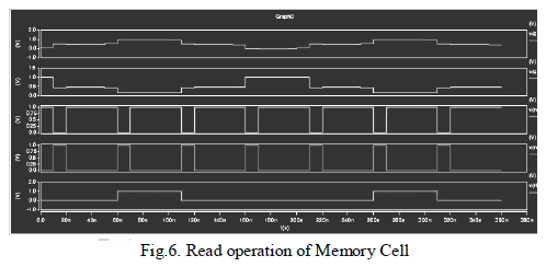
| HSPICE simulation software is used write and read operation. The write transmission gate Q1 and Q2 allows the correct data from data in to wbl to be written into the memory cell q and qb. The read operation of the proposed ternary cell is performed as follows: rbl is precharged to 1/2 Vdd prior to the read operation and the read transmission gates Q17 and Q18 are accessed to read the correct data from the memory cell. The read operation of the proposed ternary memory cell has been simulated which operates as the ternary memory cell is storing a logic “2”; then, the read bit line rbl is charged to logic “2” when the read word lines rwl and rwlb are accessed. The ternary memory cell is storing a logic “0”; the read bit line rbl is discharged to logic “0” when the read word lines rwl and rwlb are accessed. |
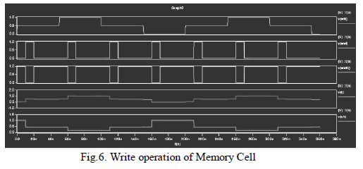 |
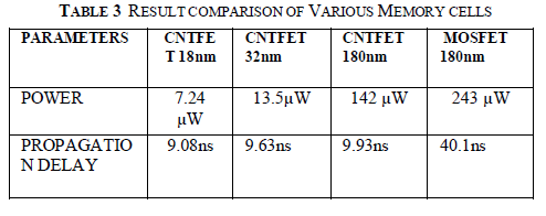
| The ternary memory cell is storing logic “1”; rbl remains at logic “1”. A ternary STI is then connected to the read bit line rbl to sense the voltage at rbl. The average power consumption is measured using HSPICE for the proposed memory cell design. The power consumption is reduced due to usage of ternary logic with CNTFET. Compared to the high-leakage nano- CMOS device, a CNTFET has a significantly smaller OFF current; so, the power consumed when the transistor is OFF is greatly reduced in CNTFET designs. The CNTFET has a significantly higher ON–OFF current ratio compared to the MOSFET in the deep submicrometer range. The propagation delay is also reduced when compared to MOSFET circuits. For MOSFET CMOS circuits the minimum distance between pull up and pull down network must be 10 λ but with CNTFET CMOS circuit the same must be 3λ so the area can be reduced though the no. of transistors increases.[21] Table 3 shows the power consumption and propagation delay of various Memory cells. |
 |
 |
VI. CONCLUSION
|
| The 3VL 6T STI is designed with 18 nm technology and their parameters are analyzed. One bit memory cell is designed using 6T STI and parameters are compared with 180nm CMOS SRAM, 180nm CNTFET memory. It is found that the power consumed by 32nm CNTFET 3VL memory is 13.5μW , which is much less than that of SRAM and other memory cell. The power consumed by the memory cell designed with 18nm CNTFET technology is found to be 7.24 μW. All together the memory cell with 18nm CNTFET is considered as the most power efficient technology among the others. Thus as the channel length reduces the power consumption is also reduced. The future work consists of designing the memory with 10nm CNTFET technology. The buffer used in the Fig5. was binary in nature it is replaced by ternary buffer which will further reduce the power. Even though the area is increased, the power reduction will compensate the area . An 8x8 bit memory array is designed with this 10nm CNTFET technology. Cross bar memories with 10nm CNTFET has interesting applications. |
References
|
- P. L. McEuen, M. S. Fuhrer, and H. Park : 'Single Walled Carbon Nanotube Electronics', Nanotechnology, IEEE Transactions on., 2002, 1, (1), pp. 78-85
- M. Mukaidono, “Regular ternary logic functions - ternary logic functions suitable for treating ambiguity,” IEEE Trans. Comput., vol. C-35, no. 2, pp. 179–183, Feb. 1986.
- K.Nepal: 'Dynamic circuits for Ternary computation in Carbon Nanotube based Field Effect Transistors', NEWCAS Conference (NEWCAS), 2010 8th IEEE International, June 2010: pp. 53-56
- J. Appenzeller, “Carbon nanotubes for high-performance electronics-progress and prospect,” Proc. IEEE, vol. 96, no. 2, pp.201–211, Feb.2008.
- H. Hashempour and F. Lombardi, “Device model for ballistic CNFETs using the first conducting band,” IEEE Des. Test Comput., vol. 25, no. 2, pp. 178–186, Mar./Apr. 2008.
- Y. Lin, J. Appenzeller, J. Knoch, and P. Avouris, “Highperformance carbon nanotube field-effect transistor with tunable polarities,” IEEE Trans. Nanotechnol, vol. 4, no. 5, pp. 481–489, Sep. 2005.
- S. Lin,Y. B. Kim, and F. Lombardi, “The CNTFET-based design of ternarylogic gates and arithmetic circuits,” IEEE Trans. Nanotechnol., vol. 10,no. 2, pp. 217–225, Mar. 2011.
- Raychowdhury A., Roy K.: ‘Carbon-nanotube-based Voltage mode multiple-valued logic design’, IEEE Trans. Nanotechnol., 2005, 4, pp. 168–179.
- (2008). Stanford University CNFET Model website Online].Available:http://nano.stanford.edu/model.php?id=23.
- J. Deng and H.-S. P.Wong, “A Compact SPICE model for carbonnanotube field-effect transistors including non idealities and its application—Part I: Model of the intrinsic channel region,” IEEE Trans. Electron. Devices, vol. 54, no. 12, pp. 3186–3194, Dec. 2007.
- J. Deng and H.-S. P.Wong, “A Compact SPICE model for carbonnanotube field-effect transistors including non idealities and its application—Part II: Full device model and circuit performance benchmarking,” IEEE Trans.Electron Device, vol. 54, no. 12, pp. 3195–3205, Dec. 2007.
- Lucasiewicz, Jan O Logice Tr´ojwarkoscioewj English translation: On three-valuedlogic, in L. Borkowski (ed.), Selected works by Jan Lukasiewicz, North-Holland, Amsterdam, 1970, pp. 87-88
- M. Kameyama, S. Kawahito, and T. Higuchi: 'A multiplier chip with multiple-valued bidirectional current-mode logic circuits', Computer., 1988, 21, (4), pp. 43–56.
- P. Keshavarzian, and K. Navi: 'Universal ternary logic circuit design through carbon nanotube technology', International Journal of Nanotechnology., 2009, 6, (10), pp. 942-953.
- Wu X., Prosser F.P.: ‘CMOS ternary logic circuits’, IEE Proc. G., Electron. Circuits Syst., 1990, 137, pp. 21–27
- 1 Wu X., Deng X.: ‘Design of ternary current-mode CMOS circuits based on switch-signal theory’, J. Electron., 1993, 10, pp. 193– 202
- T. Rueckes, K. Kim, E. Joselevich, G. Y. Tseng, C. Cheung, and C. M. Lieber: 'Carbon nanotube based nonvolatile random access memory for molecular computer', Science., 2000, 289, pp. 94–97
- Y. Li, W. Kim, Y Zhang, M Rolandi, and D. Wang, “Growth of singlewalled carbon nanotubes from discrete catalytic nanoparticles of various sizes,” J. Phys. Chem., vol. 105, pp. 11424–11431, 2001.
- Y. Ohno, S. Kishimoto, T. Mizutani, T. Okazaki, and H. Shinohara, “Chirality assignment of individual single-walled carbon nanotubes in carbon nanotube field-effect transistors bymicro-photocurrent spectroscopy,” Appl. Phys. Lett., vol. 84, no. 8, pp. 1368–1370, Feb. 2004.
- A. Lin, N. Patil, K. Ryu, A. Badmaev, L. G. De Arco,C. Zhou, S. Mitra, and H.-S. P. Wong, “Threshold voltage and on–off ratio tuning for multiple tube carbon nanotube FETs,” IEEE Trans. Nanotechnol., vol. 8, no. 1,pp. 4–9, Jan. 2009.
- Sheng Lin, Yong-Bin Kim and Fabrizio Lombardi, “Design of a Ternary Memory Cell Using CNTFETs” IEEE Transactions On Nanotechnology, vol. 11, no. 5,pp.1019-1025 Sept 2012.
- K. C. Smith, "The prospects for multivalued logic: A technology and application view," IEEE Trans Comput, vol. C-30, pp. 619- 634, Sept. 1981.
- P. C. Balla and A. Antoniou, “Low power dissipation MOS ternary logic family,” IEEE J. Solid-State Circuits, vol. 19, no. 5, pp. 739–749, Oct.1984.
- H. T. Mouftah and I. B. Jordan, “Design of ternary COS/MOS memory and sequential circuits,” IEEE Trans. Comput., vol.C-26, no. 3, pp. 281–288, Mar. 1977.
- U. Cilingiroglu and Y. Ozelci, “Multiple-valued static CMOS memory cell,” IEEE Trans. Circuits Syst. II, Analog Digit. Signal Process., vol. 48, no. 3, pp. 282–290, Mar. 2001.
- K. You and K. Nepal, “Design of a ternary static memory cell using carbon nanotube-based transistors,” IET Micro Nano Lett., vol. 6, no. 6,pp. 381–385, Jun. 2011.
- S. Lin, Y.-B. Kim, and F. Lombardi: 'A novel CNTFET-based ternary logic gate design', Circuits and Systems, 2009. MWSCAS '09. 52nd IEEE International Midwest Symposium on, Aug. 2009: pp. 435–438
|