International Journal of Advanced Research in Electrical, Electronics and Instrumentation Engineering
ISSN ONLINE(2278-8875) PRINT (2320-3765)
ISSN ONLINE(2278-8875) PRINT (2320-3765)
K.Venkata laxmi1, B.Lakshmi2
|
| Related article at Pubmed, Scholar Google |
Visit for more related articles at International Journal of Advanced Research in Electrical, Electronics and Instrumentation Engineering
In recent years power saving is one of the important thing. Domino logic circuit is power efficient cicuit,so it is widely used in variety of applications in digital design. But it has a limitation of low noise immunity and more leakage current. This problem can be solved by using keeper transistor to compensate leakage current of pull down network. The conventional keeper domino circuit reduces the performance and more power consumption due to the contention between keeper transistor and pull down network. This problem is more in wide fan in gates due to large number of leaky paths connected to the dynamic node. In this paper ,a new technique is proposed which overcomes the contention problem and reduces power dissipation and provide high noise immunity. Simulations of wide fan in gates are designed using TSMC 180nm technology with Vdd=1V at 27°c and 110°c using mentor graphics.
Keywords |
| Domino logic,dynamic node,wide fan in,noise immunity. |
I. INTRODUCTION |
| Static CMOS logic circuits with complementary NMOS pull down and PMOS pull up networks are used for the majority of logic gates in integrated circuits.static gates have limitations, area and speed especially for wide fan in gates. To overcome these issues ,we can go for pseudo NMOS logic gate, which are most common form of CMOS ratioed logic. Pull down network is same like that of static CMOS logic gate ,but the pull up network is replaced with single PMOS transistor that is grounded so it is always ON. Pseudo nmos logic circuit has a limitation of static power dissipation and weak low level at output. By combining the advantages of low power from static CMOS logic and less area from pseudo nmos logic the dynamic logic circuit is formed by introducing the clock input signal. Dynamic CMOS logic required number of transistor that is for fan in n is n+2. Dynamic circuit reduces the short circuit power dissipation but it suffers from charge sharing, charge leakage and clock skew. More over, dynamic circuits sharing the same clock cannot be directly connected. These problems are overcome with domino logic.Domino logic circuits with high fan in gates are widely used due to their high performance. Domino logic circuit is formed by adding a static CMOS inverter to the output of dynamic CMOS logic. The idea of forming domino logic is to limit charge leakage and charge sharing by feeding back the inverting output. Major drawback of domino logic circuit is more sensitive to noise than static logic families.On the other hand, Power consumption is one of the important factor in present days especially for portable devices. One way to achieve low power is scaling down the supply voltage.As supply voltage reduces, the threshold voltage (Vth) of transistors is reduced. However lowering the threshold voltage leads to an exponential increse of subthreshold leakage current. Another way to reduce power is technology scaling. As the technology scales down to nano meters, the gate oxide thickness is scaled down. Such thin gate oxide leads to significant gate leakage current. For these reasons static power consumption i.e., leakage power dissipation has become a dominant factor for current and future technologies. Reduction of leakage current and improving noise immunity is a major concern. The most popular domino logic is the standard footerless domino logic (SFLD). In this design, PMOS keeper transistor is employed to prevent undesired discharging at the dynamic node due to the leakage current and charge sharing of the pull down network,thus improving the robustness. Keeper ratio is defined as the ratio of the current drivability of keeper transistor to the evaluation network. |
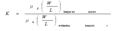 |
| Where W and L are transistor sizes, μp and μn hole and electron mobilities. Schematic of basic standard footerless keeper domino logic shown figure 1 |
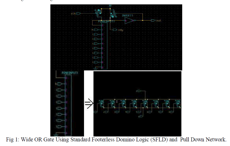 |
| Operation of domino logic occurs in 2 phases.In Precharge phase, clock signal is at low i.e,(clock =0) all the inputs at low,the dynamic node pulled up to Vdd through Precharge PMOS device. In evaluation phase, clock signal is at high i.e,(clock =1) depends on input pattern either charge of dynamic node retained or removed. If all the inputs at low,output of OR gate must be zero,hence dynamic node must remain high and consequently the pmos keeper must stay on to compensate for any leakage current drawn out of dynamic node. In the case where atleast one of the input is high, stored charge on dynamic node must be discharged. In this case both PMOS keeper transistor and pull down network circuit simultaneously ON during the time interval from when pull down network starts conducting until voltage of output node reaches a certain high voltage. The contention between keeper and pull down network increases as the keeper transistor is upsized.this causes an increases in the evaluation delay of the circuit and increase in power consumption and degrades the performance. while weak keeper is to increase speed up switching transistion. There is conflict requirement gives rise to tradeoff between power and performance. |
II. LITERATURE SURVEY |
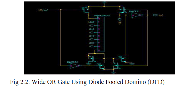
| Several domino techniques have been proposed in the literature such as conditional keeper domino logic (CKD) [2], diode footed domino logic (DFD)[3], leakage current replica keeper logic (LCR)[4], controlled keeper by current comparison domino logic (CKCCD)[5] and current comparison domino (CCD)[6] are shown in fig 2.1,2.2,2.3,2.4, respectively. The main goal of these circuits is to reduce leakage and power consuption and improve noise immunity,especially for wide fan in gates. |
| A. Conditional Keeper Domino Logic (Ckd): Another existing leakage tolerant technique is conditional keeper domino (CKD) logic[2]. schematic of CKD logic shown in figure. Conditional keeper domino logic circuit consists of 2 keeper transistors,small keeper transistor turns on in precharge phase and large keeper transistor turns ON in evaluation phase. In precharge phase when clock is low,the pull up transistor is on ,so the dynamic node charged to Vdd. |
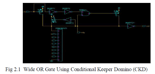 |
| At the beginning of evaluation phase when clock is high,the small keeper K1 turns on to hold the state of the dynamic node and large keeper k2 turns off for some time. This keeper transistor sized larger than keeper transistor K1 to maintain the state of dynamic node for the rest of evaluation phase to improve the robustness of the circuit. However, conditional keeper domino has some drawbacks such as increasing delays of the inverters and nand gate to improve noise immunity to the circuit. |
| B. Diode Footed Domino (DFD): |
| In diode footed domino logic [3], NMOS transistor m1 connected in diode configuration i.e, gate and drain terminals are connected together in series with the evaluation network. Diode footer transistor reduces sub threshold leakage current due to the stacking effect. Due to the leakage current of evaluation transistors, there is some voltage established across diode footer m1 in the evaluation phase. This voltage drop makes Vgs of the off evaluation transistor negative, causing an exponential reduction in sub threshold leakage. Voltage drop across diode footer increases the body effect of the evaluation transistor which also helps in reducing the sub threshold leakage. On the other hand diode footer transistor m1 increases the switching threshold voltage of the gate by the threshold of NMOS devices and hence gate switching vth is 2vth. higher switching voltages results better noise immunity. |
 |
| C. Leakage Current Replica Keeper (LCR) |
| In leakage current replica keeper [4], current mirror circuit is added to the keeper of standard footer less domino logic. Transistor m1 of the mirror circuit is connected in diode configuration, i.e, gate of the PMOS transistor is connected to the drain. By doing like this both gate and drain of the PMOS transistor is at potential voltage level of the keeper. Keeper voltage is same as the potential of drain of keeper transistor mk1. This leakage current replica keeper reduces the power consumption . |
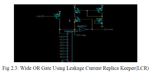 |
| Operation of circuit is as follows : In precharge phase, when clock is low and all the inputs are at low level , dynamic node charged up to Vdd. During precharge phase, output is at low which turns on the keeper transistor MK2 and it acts as a short cuircuit transistor. Now the drain of MK1 transistor is directy connected to the dynamic node and due to the diode configuration of this keeper transistor MK1 drain voltage of M1 is also at the logic low level of dynamic node. High voltage of drain of M1 transistor reduces the leakage current. In this way, the leakage power is reduced. |
| D. Controlled Keeper by Current Comparison Domino (CKCCD) |
| In CKCCD technique, keeper transistor controlled by the current comparison domino mechanism. Basic idea of this technique is that keeper transistor is controlled with the current comparison so that when dynamic node is truly discharged, keeper transistor will be off to prevent the contention between keeper transistors and pull down network. Due to this power and the propagation delay gets reduced. Schematic of CKCCD shown in figure2.4 |
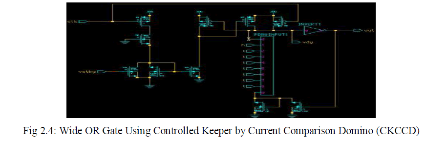 |
| leakage current is reduced due to the stacking effect because the minimum voltage of a MOS transistor in diode configuration is identical to vgs= vds= vtn.In Evaluation phase, when clock is in high level i.e, CLK=’1’, the precharge transistor and M8 are off.Depending on the inputs, other transistors may be turns on or off.First if all inputs at low level, the mirror current is larger than the PDN leakage current, the voltage node is discharged to zero This reduces the contention by turning off the keeper transistor. |
| E. Current Comparison Domino Logic (CCD): |
| In CCD logic uses pull up network (PUN) instead of Pull down network(PDN). There is a race between PUN and the reference current. Keeper transistor added in series with the reference current to reduce power consumption when voltage of the output node has fallen to the ground voltage. |
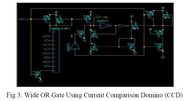 |
| Pre discharge Phase: In this phase, CLOCK is at low level i.e, CLK=’0’ and all input signals are at high level. Voltage of the dynamic node falls to low level by the transistor Mdis and raises to high level by the transistor Mpre. Therefore, the transistors Mpre, Mdis, Mk1,Mk2 are on and other transitors are off. Then the output voltage raised to high level. |
| Evaluation phase: When CLOCK is at high level CLK=’1’ and the transitors may be turns on or off depending on the input voltages. Here two states may possible, first all the inputs are high, a small amount of voltage is recognized across the transistor M1 due to leakage current. Even though the leakage current is mirrored by transistor M2, the keeper transistor of the second stage Mk1 and Mk2 give back this mirror leakage current. It is clear that upsizing transistor M1 and increasing the Mirror ratio increases the speed at cost of high noise immunity degradation. Second ,at least one input falls to low level, one conduction path exists, pull up current flow is raised and voltage of node is reduced to non zero voltage, which is equal to the gate source voltage of the saturated transistor M1. This voltage same as the drain to source voltage of M1 depend on size of M1 and its current. Increasing the pull up current increases the mirrored current in transistor M2, thus voltage of the dynamic node is charged to Vdd, yields discharging the voltage of the output node and turning off the main keeper transistor Mk1.Due to this contention between keeper and mirror transistor are mitigated. |
III. PROPOSED WORK |
| Static Evaluation Domino Logic (SEDL): |
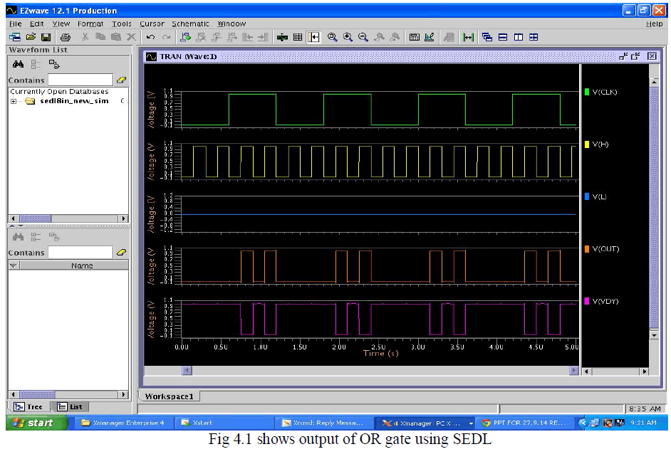
| In case of wide fan in gates, capacitance of the dynamic node is large then speed decreases severely. Due to the large parallel leaky paths, power consumption increases and noise immunity reduces due to large contention. These problems would be solved by static evaluation domino logic.SEDL works as a static gate in the evaluation network.This circuit demonstrates less power and very efficient in performance. A wide fan in OR gate using SEDL shown in fig 3.1. circuit operates in 2 phases. In precharge phase when clock is at low level, the dynamic node charges to high. NMOS transistor is in off state and it is at floating, this value passed to keeper transistor. At the beginning of the precharge phase the footer transistor is turned on, and it may pull the dynamic node to ground but because of continuing to charge in the precharge state, he voltage at the dynamic node remains high. |
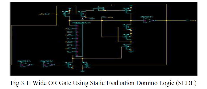 |
| In the beginning of the evaluation phase, the footer transistor is in off state because of the delay introduced. In this time slot, it allows evaluation network to perform its operation. If any of input tries to pull down the dynamic node, then the voltage between dynamic node and footer, so MN2 transistor turns on, the dynamic node pulled down to the ground. This setup is used to prevent leakage charge at the beginning of evaluation by utilizing the stacking effect. After complete delay footer transistor turns ON, it makes MN2 to turns OFF.If there is no input makes a path between dynamic node and the footer node, and at the beginning of evaluation phase footer node is at floating state. This voltage should not turn the MN2 transistor ON, so there is no discharging path from dynamic node to ground. At this moment, the output is at logic low level and makes the keeper transistor MK to give out the dynamic node in charging to its maximum. After that, if dynamic node is discharged and if any input disconnected from its operation, at this time the voltage value of dynamic node is floating , and as mentioned before it turns ON the NMOS transistor and produces a weak low logic level at the inverter output. |
IV. SIMULATION RESULTS AND COMPARISON |
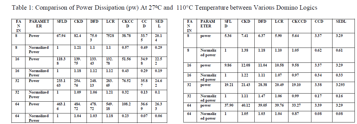
| The proposed circuit is simulated using mentor graphics in the TSMC180nm technology at 27âÃÂðc and 110âÃÂðc. The supply voltage used in the simulations is 1V. Table 1&2 shows power dissipation of SFLD and various domino logics at 27°C and 110°C. |
 |
 |
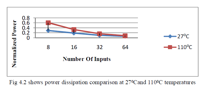 |
| Proposed SEDL logic has less power dissipation compared to the SFLD logic. As the temperature increases power dissipation also increases. |
 |
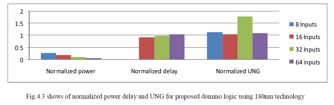 |
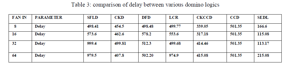
| Proposed circuit provides less power dissipation better performance and high noise tolerance compared to the various domino logics. |
V. CONCLUSION |
| Leakage current of the pull down network increases significantly with the technology scaling and reducing supply voltage especially for wide fan in gates. Along with this yields low noise immunity and more power consumption. In addition, increasing fan in not only increases delay, also increases contention between keeper transistor and pull down network. In this, new domino technique called static evaluation domino logic technique which increases noise immunity and reduce contention and power dissipation. Existing domino techniques are simulated with mentor graphics in the TSMC 180nm technology at a power supply of 1V. Results of simulations shows that the proposed circuit exhibits less power dissipation for 8, 16, 32 and 64 inputs compared to SFLD. |
References |
|