International Journal of Advanced Research in Electrical, Electronics and Instrumentation Engineering
ISSN ONLINE(2278-8875) PRINT (2320-3765)
ISSN ONLINE(2278-8875) PRINT (2320-3765)
Dr.K.Ravichandrudu1 , P.Suman Pramod Kumar2, M.Sailaja3, M.Meena3
|
| Related article at Pubmed, Scholar Google |
Visit for more related articles at International Journal of Advanced Research in Electrical, Electronics and Instrumentation Engineering
Conventional AC/DC power converters that are connected to the line through full-wave rectifier draws a non-sinusoidal input current. These Harmonic currents flowing through the impedances in the electrical utility distribution system can cause several problems such as voltage distortion, heating, noises. These harmonics distort the local voltage waveform, potentially interfering with other electrical equipment connected to the same electrical service and reduce the capability of the line to provide energy. This fact and the presence of standards or recommendations have forced to use power factor correction in power supplies. Boost regulators have been with us for many years as a power factor correction rectifiers. The main problem in boost rectifier is, the output voltage is very sensitive to Duty ratio variations. So maintaining the output voltage with in the regulation is very complex. Boost regulators are draws power from utility at unity power factor when it is operated in continuous conduction mode.
Keywords |
| Rectifier,power factor conduction mode,Modulator |
I. INTRODUCTION |
| In this Paper, the Predictive Switching Modulator(PSM) for current mode control of high power factor boost rectifier is proposed. In this strategy the duty ratio of the switch is controlled in such a way that the estimated inductor current will be proportional to the rectifier input voltage at the end of the switching period(Ts). The estimation of the inductor current is possible since the input voltage is practically constant over a switching period. This enables us to predict the current ripple of the subsequent off period during the on time of the switch itself. The input current waveform gets distorted in the Discontinuous Conduction Mode(DCM) operation of the NLC controlled boost rectifier. The advantage of the PSM is the extended range of Continuous Conduction Mode (CCM) of operation compared to the NLC. The PSM modulator has the structure of a standard current programmed controller with compensated ramp that is nonlinear. The steady-state stability condition and the low-frequency small-signal model of the PSM switched boost rectifier are derived by applying standard graphical and analytical methods of the current mode control. |
II. BASIC OPERATION OF THE BOOST RECTIFIER |
| The boost is a popular non-isolated power stage topology, sometimes called a step-up power stage. Power supply designers choose the boost power stage because the required output voltage is always higher than the input voltage, is the same polarity, and is not isolated from the input. The input current for a boost power stage is continuous, or non-pulsating, because the input current is the same as the inductor current. The output current for a boost power stage is discontinuous, or pulsating, because the output diode conducts only during a portion of the switching cycle. The output capacitor supplies the entire load current for the rest of the switching cycle. The power circuit of dc-dc Boost rectifier is shown in fig.1. |
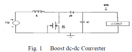 |
| When the switch is on, the diode is reversed biased, thus isolating the output stage. The input supplies energy to the inductor. When the switch is off, the output stage receives energy from the inductor as well as from the input. |
| The steady state analysis for continuous conduction and discontinuous conduction mode of operation is explained below. |
| A. Boost Power Stage Steady-State Analysis |
| A power stage can operate in continuous or discontinuous inductor current mode. In continuous inductor current mode, current flows continuously in the inductor during the entire switching cycle in steady-state operation. In discontinuous inductor current mode, inductor current is zero for a portion of the switching cycle. It starts at zero, reaches a peak value, and returns to zero during each switching cycle. The output filter capacitor is assumed to be very large to ensure a constant output voltage V0(t)≈V0 |
| B. Boost Steady-State CCM Analysis |
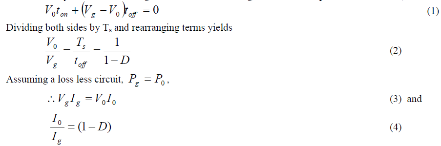
| The basic power circuit of boost converter during ON and OFF period is shown in Fig.2 Fig.3.shows the steady-state waveforms for this mode of conduction where the inductor current flows continuously [ i (t) > 0 l ]. |
| Since in steady state the time integral of the inductor voltage over one time period must be zero, |
 |
 |
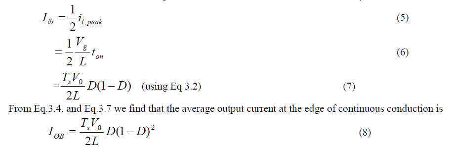
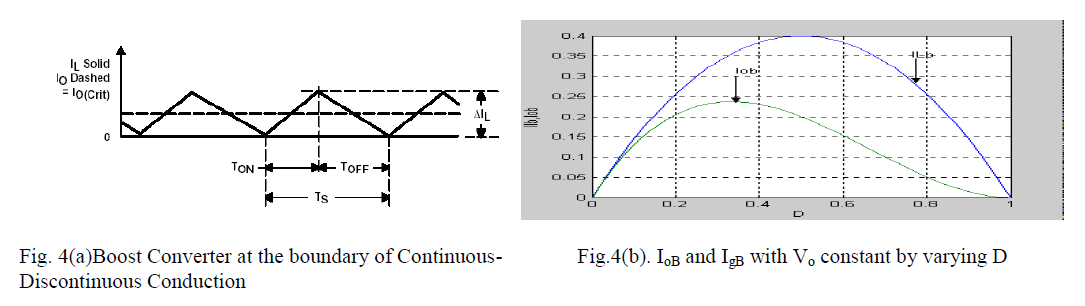
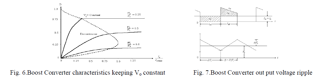
| C. Boundary Between Continuous and Discontinuous Conduction |
| Fig.4(a).Shows the waveforms at the edge of continuous conduction. By definition, in this mode i1 goes to zero at the end of the off interval. The average value of the inductor current at this boundary is |
 |
 |
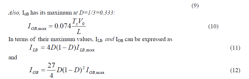 |
| Fig.4(b) shows that for a given D, with constant V0, if the average load current drops below IOB (and, hence, the average inductor current below ILB), the current conduction becomes discontinuous. |
| D. Discontinuous conduction mode |
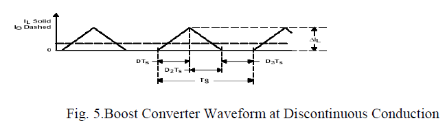 |
| In Fig.5 The discontinuous current conduction occurs due to decreased P0 and ,hence, a lower IL, since Vg is constant. Since IL peak is the same in both modes in Fig3.4 , and Fig.5. a lower value of IL is possible only if V0 goes up in fig.5. |
| If we equate the integral of the inductor voltage over one time period to zero, |
 |
| it is more useful to obtain the required duty ratio D as a function of load for various values of g V V 0 . By using Eqs… , we determine that |
 |
 |
| are transferred from the input to the output capacitor and to the load. If the load is not able to absorb this energy, the capacitor voltage V0 would increase until an energy balance is established. |
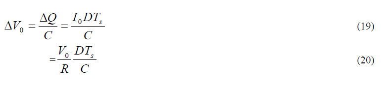
| E. Output Voltage Ripple |
| Therefore, the peak-peak voltage ripple is given by |
 |
| F. Controlling Of Boost Rectifier |
| The various methods of power factor Correction can be classified as |
| (i) Passive Power Factor Correction techniques |
| (ii) Active Power Factor Correction techniques |
| 1. Passive Power Factor Correction Techniue |
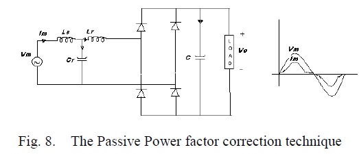 |
| In this approach an L-C filter is inserted between the AC mains line and the input port of the diode rectifier of AC-to- DC converter as shown in Fig.8. This technique is simple and rugged but has bulky size and heavy weight and the Power Factor can not be very high. |
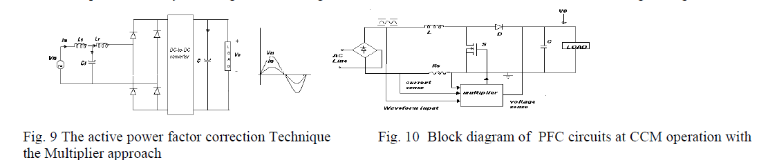
| 2. Active Power Factor Correction Technique |
| The Power Factor can reach almost unity and the AC/DC interface of power converter emulates a pure resistor as shown in Fig.9. Comparing with the Passive Power Factor Correction methods, the Active Power Factor Correction techniques have many advantages such as, High Power Factor, reduced Harmonics, small size and light weight. |
 |
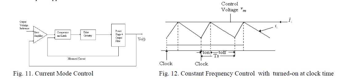 |
| There are two basic controllers are proposed for the PWM power factor correction technique, namely, Peak current mode control and Average current mode control to boost converter operating in CCM . |
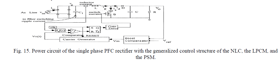
| 3. Peak Current Mode Control: |
| This technique was proposed for boost converter operating at CCM mode with constant switching frequency as shown in fig. 13. It has all he advantages of the boost type configuration working at CCM mode. Te problem of this technique is its requirement of a slope compensation to stabilize the control system. |
 |
| 4. Average Current Mode Control |
| This technique was proposed for boost converter operating at CCM mode with constant switching frequency, as shown in fig. 14. It has all the advantages of the boost type configuration working at CCM mode. The demerit of this technique is current control system is complex and difficult to analyze and synthesize. In a simplified circuit was proposed to shape the sinusoidally varying average current without sensing the input voltage. |
| However, The peak current mode controller and average current mode controllers are suffering from the stability problem due to the presence of inherent sub harmonic oscillations if the duty ratio of the power switch is greater than 50% and noise immunity. |
 |
| 5. Quasi Steady-State Approach |
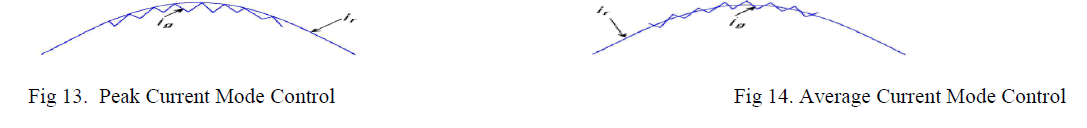
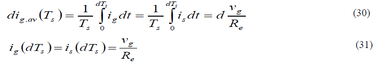
| The line frequency in Fig.3.6. is usually well below the switching frequency, hence, the input voltage of the dc-dc converters can be approximated as a constant in a consecutive switching periods.. The important property of the quasi steady state operation is that all quantities can be approximated with their steady-state values. |
| The control objective of the resistor emulator is to force the input current of the dc-dc converter to be proportional to the input voltage so that the input impedance is resistive. In other words, the local average of the input current |
 |
| Vo is a constant over a line cycle if the output capacitance is large enough; therefore, if vm is also a constant in line cycle, <ig> is proportional to vg and the emulated resistance |
| Voltage vm regulate Re so as to control the input current. |
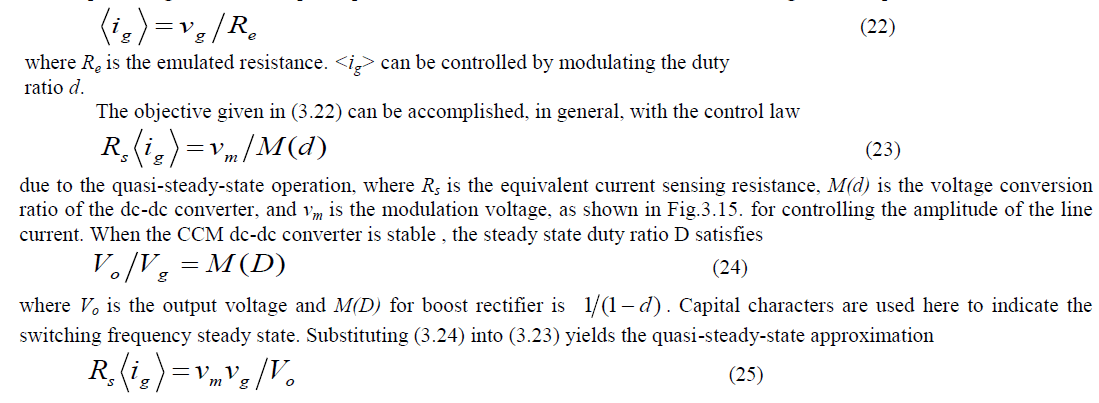
III. PREDICTIVE SWITCHING MODULATOR( PSM) |
| The generalized control objective of a high power factor boost rectifier can be expressed as |
 |
| Re is the emulated resistance of the rectifier and is a function of the inductor current . This function can be different for different control strategies. For example NLC implements average current mode control, so for NLC (3.27) is the specific expression of f(ig) |
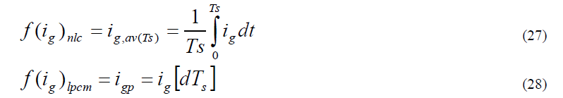 |
| In the proposed modulator the duty ratio of the switch is controlled in such a way that the inductor current becomes proportional to the rectified input voltage at the end of each switching period. Therefore for PSM the function is given by |
 |
| Fig. 3.16 shows the generalized control objective of the boost rectifier. |
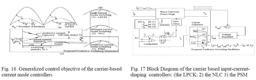 |
| Operating principle of the PSM. |
| For a boost rectifier the switch current is equal to the inductor current during ON time of the switch. In a switching period Ts, instead of the inductor current, it is convenient to average the switch current by carrying out integration only over the ON time of the switch because the switch current is zero during the rest of the period. Therefore the modulator of NLC implements the control law given by (28). For LPCM and PSM either the switch current or the inductor current can be sensed. The control laws for LPCM and PSM in terms of the switch current are given by |
 |
 |
| It may be noted that the inductor current at the end of period is equal to the current at the beginning of the next |
 |
| of the input voltage when the converter is operating in CCM the slope of the turn-off current can be predicted during ON time of the switch itself. Then instead of (32), (33) can be used for PSM |
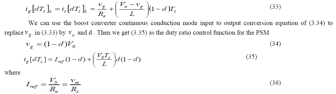 |
| Rs is the current sense resistance of the converter and vm is the input voltage to the modulator. Under closed loop operation is obtained as the output of the voltage error amplifier loop. In nlc and lpcm, the right-hand-side expressions of (3.27) and (3.28) are converted into suitable carrier waveforms by replacing the duty ratio term d by s t T . Similarly the carrier waveform I (t) c for the predictive switching modulator can be expressed as |
 |
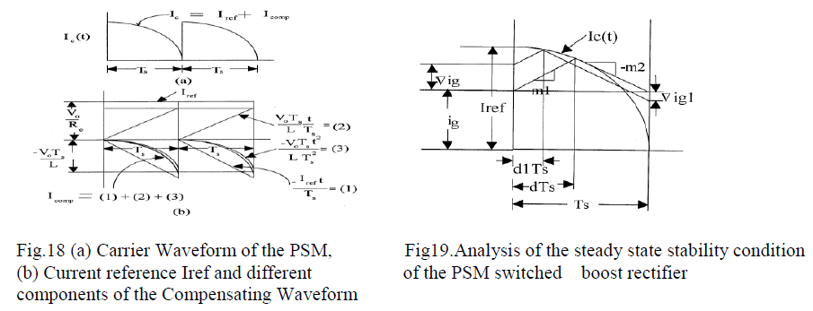
| Steady state stability condition |
| steady-state stability analysis presented in this section is Graphical in nature. have For deriving the steady-state stability condition for the current mode controlled dc–dc converter, the objective is to quantify the steady-state stability condition of the PSM switched boost rectifier in terms of circuit parameters and switching frequency of the converter. |
| The steady-state carrier waveform, shown in Fig. 18(a), is configured as a function of d=t/Ts, in the standard structure of |
 |
 |
 |
 |
| From (3.50) and (3.51), the steady-state stability condition for the PSM switched boost rectifier in terms of circuit parameters can be expressed as |
 |
| B. Discontinuous conduction mode (DCM) |
| In the DCM, the inductor current is zero at the beginning In the DCM, the inductor current is zero at the beginning of a switching period. Therefore the duty ratio of the period is determined by the modulator equation |
 |
| But in DCM,(3.34) is no longer valid. Instead |
 |
 |
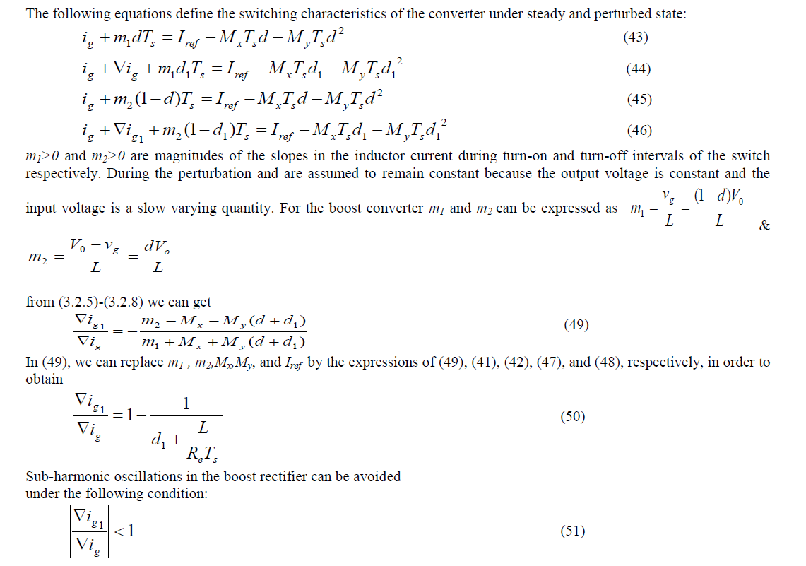
| Kcp, Kcn and ,Ksp and as functions of Mg are plotted in Fig. 3.20. Kspvalues are valid only in the range in which CCM operation occurs, because such a condition has been used in its derivation. |
IV. LOW FREQUENCY SMALL SIGNAL MODEL FOR PSM |
| In this section, we would like to develop a linear, low-frequency, small-signal model of the boost rectifier switched by the PSM In a line cycle, the rectified input voltage varies from 0 to vgm. Under steady-state condition the inductor current Ig is proportional to rectified input voltage and the volt-second balance for the boost inductor occurs at every switching period (Ts). |
| The state space averaged model of the boost converter power stage is given by (26). We have used that model at the dc operating point of input voltage rms |
 |
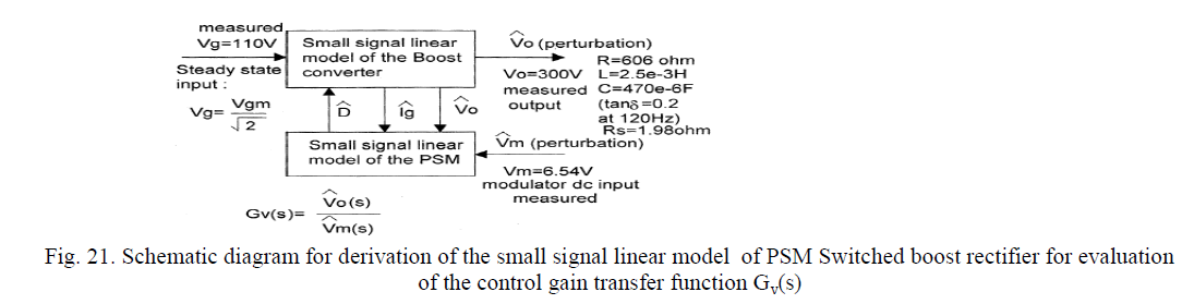 ` ` |
| The modulator uses the inductor current Ig and the output voltage V0 for producing the duty ratio of the period according to |
 |
 |
| The analytical model developed in this section is valid at any input–output and load condition as long as the boost converter operates in the continuous conduction mode. |
 |
| Fig. 22shows the Bode plot of the control gain transfer function that is obtained by analysis. The dc input voltage of the modulator is Vm=6.54v. It produces an output voltage of V0=300v, at Vg =110v and at load resistance of R=606Ω. |
| The control gain transfer function of nlc is first order that can effectively be used to design the frequency response of the voltage error amplifier. Usually for power factor correction circuit the closed loop bandwidth is chosen around 5–10 Hz. Therefore the small-signal model developed here, even though accurate for higher frequency of operation compared to that of dc-dc boost converter, has no added advantage so far as the design of the closed loop controller is concerned. |
V.CONCLUSION |
| Boost regulator with predictive switching modulator works for high power ratings and extended range of continuous conduction mode operation. |
VI.SIMULATION RESULTS |
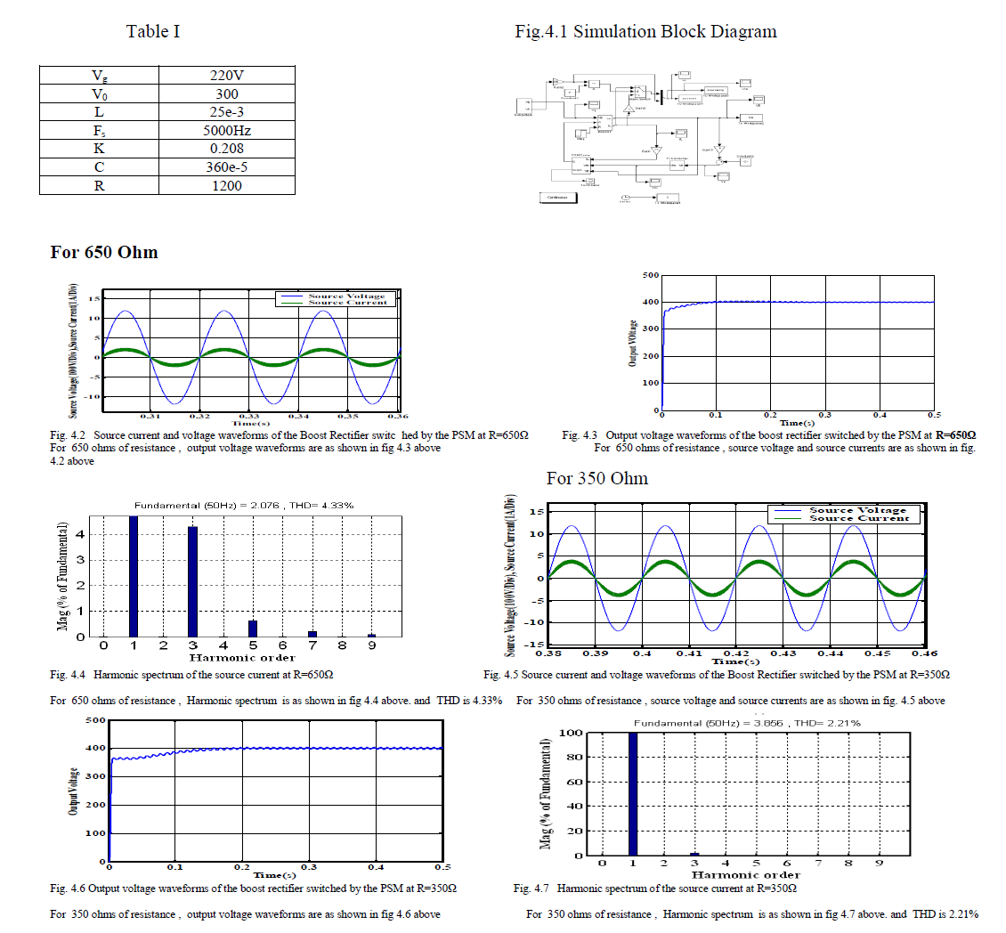
| The Simulation work is done by using MATLAB/Simulink. The simulation diagram for the PFC Boost rectifier with PSM is shown in Fig.4.1. simulation result of the input current waveform is shown with the component values given by Table I. Form the Fig.4.2 by using the PSM we can get the THD in input current waveform is 6.08% |
 |
References |
|