Keywords
|
| Multibit flips Flop, Integrated Clock Gating Circuit, Optimal Clusters, Data-Driven Clock Gating. |
INTRODUCTION
|
| The introduction of integrated circuits (ICs), commonly referred to as microchips or simply chips, was accompanied by the need to test these devices. Small-scale integration (SSI) devices, with tens of transistors in the early 1960s, and medium scale integration (MSI) devices, with hundreds of transistors in the late 1960s, were relatively simple to test. However, in the 1970s, large-scale integration (LSI) devices, with thousands and tens of thousands of transistors, created a number of challenges when testing these devices. In the early 1980s, very-large-scale integration (VLSI) devices with hundreds of thousands of transistors were introduced. Steady advances in VLSI technology have resulted in devices with hundreds of millions of transistors. |
| One of the major dynamic power reduced by clock gating method in computing and consumer electronics products in the overall system’s clock signal then reduce the 30%–70% of the total dynamic power consumption [2] and then reduce the overall circuit power to reduce15- 20% of Grouping Flip Flop data driven clock gating method [1].Clock gating is major method of educing clock signal. Generally, when a logic unit is clocked, it is based on the sequential elements receiving the clock signal, sequentially they will toggle in the next cycle whether it is required or not. The data driven clock gating circuit using clock enabling signals are manually added for every FF as a part of a design methodology [1]. |
| With clock gating, the clock signals are ANDed with explicitly predefined enabling signals. Clock gating is employed at all levels of system architecture, block design, logic design, and gates. Several methods to take advantage of this technique are described, with all of them depending on various heuristics in an attempt to increase clock gating opportunities[7]. With the rapid increase in design complexity, computer aided design tools supporting system-level hardware description have become commonly used. Although substantially increasing design productivity, such tools require the employment of a long chain of automatic synthesis algorithms, from register transfer level (RTL) down to gate level and net list [8]. Unfortunately, such automation leads to a large number of unnecessary clock toggling, thus increasing the number of wasted clock pulses at flip-flops (FFs) as shown in this paper through several industrial examples. |
| In this paper, a model for data-driven gating is developed based on the toggling activity of the constituent FFs. The optimal fanout of a clock gater yielding maximal power savings is derived based on the average toggling statistics of the merging FFs, process technology, and cell library in use [10]. In general, the state transitions of FFs in digital systems depend on the data they process. Assessing the effectiveness of data-driven clock gating requires, therefore, extensive simulations and statistical analysis of the FFs activity. Another grouping of FFs for clock switching power reduction, called Multibit FF (MBFF). MBFF attempts to physically merge FFs into a single cell such that the inverters driving the clock pulse into its master and slave latches are shared among all FFs [5]. MBFFs the advantages are: 1) smaller design area due to shared clock drivers and less routing resource 2) Less delay and less power of clock network due to fewer clock sinks 3) Controllable clock skew because of common clock and enable signals for the group of flipflops and reduced depth of a clock tree [4]. |
DATA DRIVEN CLOCK GATING
|
| A data-driven clock gating circuit is shown in Fig. 1. By XORing gate its output with the present input of Integrated Clock Circuit that will appear at its output in the next clock cycle, an FF checks whether its state is subject to change, thus finding out whether its clock can be disabled in the next cycle. The outputs of k XOR gates are ORed and then latched to generate a joint gating signal for k FFs. The combination of a latch With AND gate is called Integrated Clock Gate (ICG), commonly used by industrial electronic design automation (EDA) tools. |
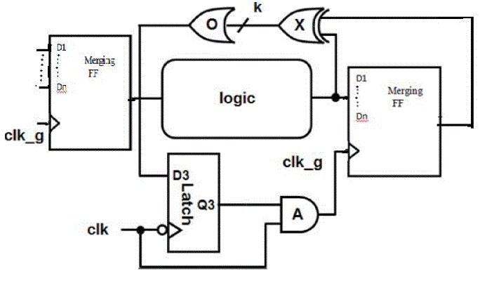 |
| Fig. 1 Circuit diagram of practical Data Driven Clock Gating |
| The practical Data Driven Clock Gating block diagram is given above. The function of module list is given that State Change Detector, Multi-Bit Flip-Flops and Integrated Clock Gating. |
| a. Clock Gating |
| Clock gating circuit is power consumed by 50 % of dynamic power. The clock gating reduce dynamic power by combinational logic circuit and then the circuit reduce clock pulse and sharing the clock signal in merging flip-flops and reduce clock signal. The profitable EDA tools are supported clock gating technique. There are two types of clock gating technique. They are Latch-based clock gating and Latch-free clock gating. The latch-free clock gating technique uses a simple AND or OR . The latch-based clock gating technique is a level-sensitive. In this project using in latchbased clock gating technique. The latch-based clock gating technique is called Integrated Clock Gate (ICG). The Integrated Clock clock will be disables in the next cycle by XORing the output of the present data input and it will reveal at the output in the next cycle. Then the output of the XOR gates are ORed for generating the gate signal for the FF’s which is to be used to avoid the glitches. The Integrated clock gate (ICG) can be used by the environmental tools by the combination of LATCH with the AND gate. These latches could be used in ultra-low power applications for a digital filter. The data driven clock gating signal are being used as an enabling signals in this applications. There will be a trade-off for ICG is the number of clock pulses could be disabled. The pulses could also be a trade-off for the hardware over-head. While increase the number of flip-flops the hardware overhead decreases to obtain by ORing the enable signals. The level of this high and the low state of signals could be processed in the same versa to give the proper output. |
| b. Multi-Bit Flip-Flops |
| Multi-Bit Flip-Flops is an effective method to reduce clock power consumption. Multi-Bit Flip-Flops can significantly reduce the number of individual loads on the clock tree, reducing overall dynamic power used in the clock tree. Area and leakage power saving can also be achieved simply by sharing the clock inverters in the flip flops with a single structure. Multi-Bit Flip-Flops provide a set of additional flops that have been optimized for power and area with a minor trade-off in performance and placement flexibility. The Flip flops share a common clock pin, which decrease the overall clock loading of the N Flops in the Multi-Bit Flip-Flops cell, reduces area with a corresponding reduction in leakage and reduce dynamic power on the clock tree significantly. |
| c. State Change detector |
| State Change detector is detecting the high state or low state. The high state is denoted by ‘1’and low state is denoted by ‘0’. The state change modification process depends on the outputs of merging FFs and combinational logic outputs. State Change detector module made up-off XOR gate and OR gate. |
PERFORMANCES OF PROJECT
|
| In data driven clock gating methodology is used to reduce the power consumption and reduce the delay of the circuit. The data driven clock gating is power reducing using in merging flip flop and integrated clock gating circuit. The block diagram of merging flip flop using data driven clock gating circuit is shown in fig 2. The ICG is disable then the output of state change detector is input of the ICG circuit. State change detector is XORed output and k enabling signal of the Flip Flop, by ORed the input of ICG circuit. The arithmetic circuit is used by logic circuit of data driven clock gating circuit. The merging Flip-flop reduces the unwanted clock signal of circuit. The unwanted glitches are reduced in data driven clock gating circuit. |
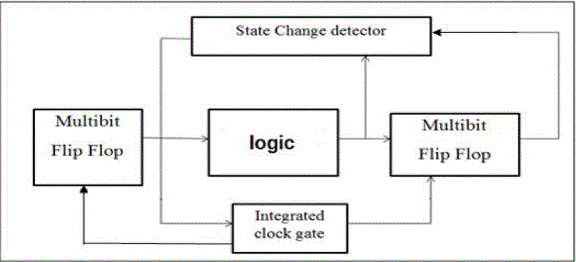 |
| Fig. 2 Block diagram of merging flip flop using data driven clock gating |
RESULT AND DISCUSSION
|
| The SYNTHESIS RESULTS of GROUPING FF USING DATA DRIVEN CLOCK GATING using is Xilinx power analyser. Grouping Flip Flop using data driven clock gating Xilinx power report shown in Fig 3. |
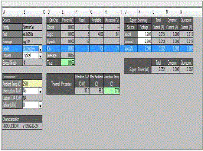 |
| Fig. 3 Grouping Flip Flop Using Data Driven Clock Gating Synthesis results- Xilinx Power Report |
| The synthesis result of Merging Flip flop Using Data Driven Clock Gating using is Xilinx power analyser. Merging Flip Flop using data driven clock gating Xilinx power report shown in Fig 3. |
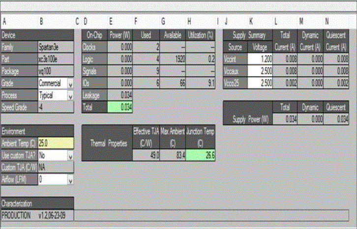 |
| Fig. 4 Merging FFs using data driven clock gating -Xilinx power |
| Table 1. Comparison of Grouping FFs using Data Driven Clock Gating Vs Merging FFs using Data Driven Clock Gating |
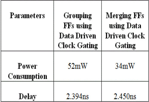 |
| The comparison of Grouping FFs using Data Driven Clock Gating Vs Merging FFs using Data Driven Clock Gating shown in table 1 the power and delay are measure by Xilinx power analyser. |
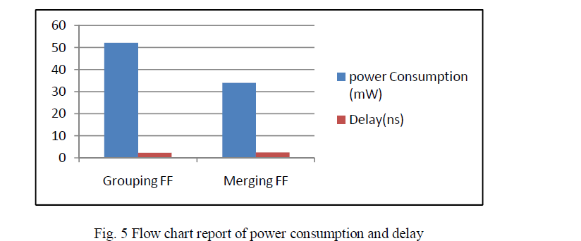 |
| The Flow chart report of power consumption and delay in Grouping FFs using Data Driven Clock Gating Vs Merging FFs using Data Driven Clock Gating shown in fig 5. |
CONCLUSION
|
| The objective of the system is to reduce the area, delay & power of data driven clock gating technique. In proposed method using merging FFs for combined clocking by a shared gater to yield highest dynamic power savings. Analysed, the results of grouping and merging FFs architectures, simulation and synthesis. As the result of the area, delay parameters, grouping FF using data driven clock gating is more effective than the merging FF using data driven clock gating. In case of grouping FFs using data driven clock gating is 30% extraordinary power saving for merging FFs using data driven clock gating. |
| In this paper, analysis between grouping FFs using data driven clock gating and merging FFs using data driven clock gating. Furthermore, real time application of DSP cores, a network processor control block, and a 3-D graphics accelerator using in merging FFs using data driven clock gating in an attempt to yield further power savings. |
References
|
- ShmuelWimer, Israel Koren (2014)“Design Flow for Flip-Flop Grouping in Data-Driven Clock Gating” IEEE TRANSACTIONS ON VERYLARGE SCALE INTEGRATION (VLSI) SYSTEMS, VOL. 22, NO. 4,
- S.Murugan(April, 2014), “Clock Power Reduction Using Merged Flip Flops Technique” IJESRT ISSN: 2277-9655.
- K. Madhanmohan, R. Murugasami(2014)“Dual Optimized System for Flip-Flop Grouping Using Data Driven Clock GatingApproach”IJARCSSE.
- S.TamilSelvi, P.Sukumar(2014) “Power Reduction for Sequential Circuit using Merge Flip-Flop Technique”International Journal of EmergingTechnology and Advanced Engineering,Volume 4, Issue 2, February 2014
- D. Gayathri, S.Giridharan, L.JubairAhmed(2014) “A Novel Approach to Reduce Clock Power by Using Multi Bit Flip Flops” InternationalJournal of Engineering Science and Innovative Technology (IJESIT) Volume 3, Issue 1.
- ShmuelWimer (sep2013), “On optimal flip-flop grouping for VLSI power minimization” ELSEVIER vol 41, ISSUE 5.
- PadminiG.Kaushik, Sanjay M.Gulhane2, Athar Ravish Khan( March 2013) “Dynamic Power Reduction of Digital Circuits by Clock Gating”Vol. 4, No. 1IJoAT
- S. Wimer and I. Koren(Oct. 2012), “The Optimal fan-out of clock network for power minimization by adaptive gating,” IEEE Trans. VeryLarge Scale Integr. (VLSI) Syst., vol. 20, no. 10, pp. 1772–1780.
- L. Benini, A. Bogliolo, and G. De Micheli,( Jun. 2010) “A survey on design techniques for system-level dynamic power management,” IEEETrans. Very Large Scale Integr. (VLSI) Syst., vol. 8, no. 3, pp. 299–316.
- V. Kolmogorov (Jan. 2009), “Blossom V: A new implementation of a minimum cost perfect matching algorithm,” Math. Programm.Comput.vol. 1, no. 1,pp. 43–67, C.
- A. Farrahi, C. Chen, A. Srivastava, G. Tellez, and M. Sarrafzadeh(Jun. 2008)“Activity-driven clock design,” IEEE Trans. Comput.-AidedDesign Integr. Circuits Syst., vol. 20, no. 6, pp. 705–714.
- W. Shen, Y. Cai, X. Hong, and J. Hu(2008,), “Activity and register placement aware gated clock network design,” in Proc. Int. Symp. Phys.Design, pp. 182–189.
- W. Shen, Y. Cai, X. Hong, and J. Hu(Mar. 2007), “Activity-aware registers placement for low power gated clock tree construction,” in Proc.IEEE Comput.Soc. Ann. Symp. VLSI, pp. 383–388.
- Chunhong, K. Changjun, and M. Sarrafzadeh(2002), “Activity-sensitive clock tree construction for low power,” in Proc. Int. Symp. Low PowerElectron. Design, pp. 279–282.
- S. Radhiga, B. Rajnivas, Dr.P.Poongodi, “DESIGN FLOW FOR CLOCK LOAD REDUCTION IN FLIP-FLOP’S USING CPSFF”IJIRTS ISSN:2321-1156, VOL 2, NUM 2.
- M. Muller, S. Simon, H. Gryska, A. Wortmann, S. Buch, Low power synthesizable register files for processor and IP cores, Integr. VLSI J. 39(2006) 131–155.
|