INTRODUCTION
|
| The main drawbacks of silicon solar cells are less efficiency and high cost. The efficiency of the solar cell mainly depends on the band gap and the reflectance of the surface. With silicon solar cells, 70% of the energy is lost as heat. Thin film solar cells reduce the manufacturing cost but their absorption power is poor. To improve the efficiency nano structured organic (plastic) and inorganic solar cells were proposed. These polymer cells were widely preferred for PV systems as their cost of production is very less moreover they can be easily handled outside clean room and also applied to many different surfaces[1,2]. Here an intermediate layer or coatings of material like silver or CIGS is given to maximize contact area of the p-n junction and to increase the light absorption capacity of the cell. |
| Since their discovery, doped conjugated polymers have been utilized in various applications like electrophotographic imaging, optical sensors, transistors, biomaterials, conductive electrodes, corrosion protection agents, lasers, LEDs, and, of course, PV cells. In the PV cell industry, device structure is absolutely vital to performance because polymeric properties are affected by the method of construction and by the presence or absence of other organic semi-conductors. Many researchers are currently utilizing a charge transfer (CT) state in blended polymers in order to maximize absorption of polymers in the near infrared regions (NIR). |
| Although polymers have potential as components for dynamic and efficient solar cells, they have several drawbacks. While the ease of chemical and electronic modification is a major advantage, it can be a minor inconvenience as the polymers must be encapsulated to maintain their desired properties[3,4]. The main problem is that polymers have low carrier mobility due to their amorphous structure. This means big problems for exciton separation and major damage to competitive power conversion efficiencies. To overcome these problems, hybrid solar cells were developed which are a combination of a polymer and nano organic or inorganic semiconductor. The objective of this paper is to highlight, and understand the applications of CdSe and TiO2 based hybrid solar cells. |
RELATED WORK
|
| The work done by Ruani et al found a new means of maximizing contact area between p and n type materials. The co-sublimation technique creates a rough surface interface with embedded microdomains that has a lower band gap, which relaxes the coupling between the electron-hole pair. Also the surface area between micro-domains is larger than a conventional p-n junction. This increase in surface area creates more opportunities for excitons to separate and be collected before recombining, allowing for potentially higher power-conversion efficiencies. In 1996, Greenham et al. reported the first polymer/nanocrystals solar cell made by dispersing CdSe or CdS nanocrystals into the conjugated polymer, MEH-PPV . The best efficiency cells were obtained by using a 90wt% (weight ratio) nanocrystals, with a corresponding volume ratio around 50%.Paul Alivisatos’ has focused on a hybrid solar cell made of cadmium selenide (CdSe) and the semi crystalline polymer, poly(3-hexylthiophene),P3HT. Takahashi et al. demonstrated that the resistivity of TiO2 thin films could vary by more than an order of magnitude depending on the measurement ambient. The lowest resistivity was observed in a hydrogen (reducing) ambient, consistent with the properties of an n-type semiconductor. |
HYBRID SOLAR CELLS
|
| To overcome the problems of the conventional Si based solar cells, hybrid solar cells were developed. These cells are a combination of a polymer and nano organic or inorganic semiconductor. Hybrid solar cells combine the excellent electronic properties of inorganic molecules with the reduced cost and flexibility of amorphous substrates . In order to achieve high hybrid solar cell performance, the electron and hole mobility's should be balanced and optimized. CdSe is a promising photovoltaic material because of its high absorption coefficient and nearly optimum band gap energy for the efficient absorption of light and conversion into electrical power[5,6]. |
CdSe based hybrid solar cells
|
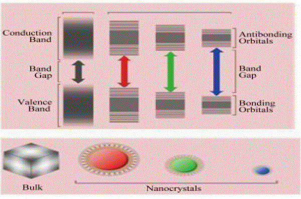
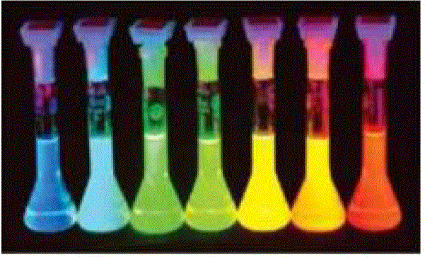
| Hybrid solar cells are similar to conventional solar cells, but in this case, nanoscale CdSe acts as the electron receptor while P3HT acts as the hole receptor. P3HT was chosen due to the fact that it has the highest hole mobility in conducting plastics available today, while the inorganic semiconductor CdSe has a high electron mobility. High mobilities ensure fast charge transport and separation of the electron-hole pair, reducing current losses due to recombination and increasing the efficiency of the cell. Electrons and holes are exchanged at the interaction surface between CdSe and P3HT. Since an electron’s position and direction can only be described by a probability, or wave function, the particular path that an electron will take is indeterminate. In an effort to direct the electron’s path, the shape of the CdSe is long and narrow, like a wire, providing a directed, low-resistance path for the electron to follow. The nanorods may also be tuned to absorb different frequencies of light. The diameter of the rod determines the band gap, where smaller diameters absorb higher frequencies of light and larger diameters absorb lower frequencies as shown in Figs.1 &2. Alternatively, the length of the rods, is proportional to the efficiency of the cell. It was found that electron transport exhibited in the shorter nanoparticles is dominated by inefficient hopping, while band conduction is more prevalent in the longer particles[7-8]. |
| From Figs. 1 &2 , it is observed that the size of CdSe nanoparticles plays very important role in fluorescence. The band gap and also the light emitted varies with the change in size of CdSe Nanoparticles. Hence the particles to be chosen are quantum dots or rods of different lengths can be decided depending on the application and its requirement. |
| CdSe thin films are well known for their applications as an optoelectronic material in solar cells and photodetectors. They are also used in the fabrication of optical filters, multilayer LEDs, photodiodes, phototransistors, etc. |
| Heterojunction solar cells with a wide band gap window and a narrow band gap absorber are currently becoming the focus of intensive research so as to develop efficient, stable and low-cost cells. Cadmium selenide, with a band gap of 2.03 eV, is an ideal material for use as the window layer of heterojunction solar cells. |
| In an effort to increase efficiency, it is important to increase the absorption of sunlight in the red part of the spectrum. While adjusting the diameter does allow the tuning of the band gap somewhat, it is also important to keep a high aspect ratio (ratio of length to diameter) so that the path of the electrons is directed. Without a high aspect ratio, the electron transport will result in the inefficient hopping . Another means of increasing the amount of absorption in the red part of the spectrum is by switching to other inorganic semiconductors like cadmium telluride(CdTe). Charge recombination also needs to be reduced to further increase efficiency. Increasing carrier mobility's reduce carrier densities, thereby lowering the likelihood of recombination. Enhancement of carrier mobility could be achieved by removing surface traps from the nanorod/polymer interface. This involves aligning the nanorods perpendicular to the substrate and further increasing their length. |
| Although CdSe/P3HT solar cells have shown promising efficiencies, Cd is a toxic heavy metal and Se is also toxic in large quantities. To solve this problem, various hybrid solar cells have been reported using zinc oxide (ZnO) and TiO2 nanocrystals. In 2004, Kwong et al. studied hybrid films consisting of TiO2 nanocrystals and P3HT with different concentration of TiO2 nanocrystals and different solvents. ZnO and TiO2 are non-toxic materials and have wide band gaps which only absorb deep violet; therefore, the efficiencies of ZnO/polymer or TiO2 /polymer solar cells are not as good as CdSe/polymer solar cells[9]. |
| Colloidal semiconductor quantum dots (QDs), made of cadmium selenide (CdSe) capped with a thin layer of higher band-gap material, zinc sulphide (ZnS), have unique optical properties. Emission characteristics of CdSe/ZnS coreshell QDs strongly depend upon the size of the CdSe core. Changes in size and size distribution of the QDs also changes the luminescence intensity and optical properties of the synthesized nanocrystals. CdSe quantum dots can also be used for supplement of dye or other quantum dots such as CdS to increase the efficiency of photovoltaic cells. CdSe have recently been reported for possible use as a photo sensitizer absorbing photons on TiO2 but the efficiency was low compared to desensitized solar cells. |
TiO2 Hybrid Solar Cells
|
| Recently, nano crystals has paved a new route for photovoltaic application due to its high surface area to volume ratio and tunable light absorption. One such application of nano crystals is titanium dioxide (TiO2 ) nano particle based solar cell. This cell utilizes high surface-area-to-volume ratio TiO2 nano crystals to increase the exciton dissociation area. These are n-type semiconductors that have a strong absorption peak in the ultraviolet, but are transparent to visible light. They have a wide band gap of 3.05-3.5 eV. Single crystal titanium dioxide TiO2 has a resistivity of about 1013 Ωcm at room temperature and about 107 Ωcm at 250?C. |
| Additionally, TiO2 nanostructures may be cheaply synthesized in a modest chemistry lab via sol gel processing [10,11]. TiO2 nanoparticles are also effective photo catalysts for treatment of air and water pollutants. Inorganic semiconducting nanoparticles are preferred in photovoltaics because of improved light gathering properties as compared to conventional thin film PV cells. The total surface area of a collection of nanoparticles embedded in a polymer matrix is much larger than the contact area of the p-n junction in conventional devices. Additionally, the spherical geometry of particles allows for absorption of light with any angle of incidence, whereas conventional thin film systems have a maximum efficiency at incident angles close to the normal of the junction. |
| Several researchers have shown interest in the optical properties and low cost of TiO2 nanoparticles for use in photovoltaic systems. A group at the Ecole Polytechnique University in Lausanne, Switzerland has achieved 10% efficiency with a new form of photovoltaic cell where a porous network of TiO2 nanoparticles is sandwiched between two electrodes. Since TiO2 nanoparticles are transparent, they do not absorb visible light efficiently. Therefore a photosensitive liquid dye, known as a sensitizer, is added to the network to improve absorption in the visible range. Additionally, an electrolyte is required to return the electrons from the cathode to the dye molecules. |
| TiO2 exists in nature as the minerals rutile, anatase, and brookite. Titanium dioxide of the rutile form is a relatively abundant mineral, however anatase and brookite are extremely rare in nature.TiO2 thin films are generally amorphous for deposition temperatures ≤ 350?C, above which anatase is formed. The most stable crystalline phase, rutile, is formed at temperatures greater than about 800?C. The brookite phase is rarely observed in deposited thin films. The functional properties of TiO2 films, powders and ceramics are strongly dependent on the phase of the material. For many applications, the size of crystals that are present also alter the behaviour of the film. The properties of TiO2 are: |
| • High Electrical resistance |
| • High durability |
| • High refractive index |
| • Good chemical resistance and high chemical stability |
| Titanium dioxide solar cell has the potential to reach low costs in future power applications compared to the conventional Si based solar cell. Depending on the cell design, a TiO2 dielectric film can serve as an anti-reflection coating (ARC), a mask for electro less metal plating, a film compatible with oxide passivation, a dopant source for emitter diffusions and a diffusion barrier to phosphorus diffusion[12]. The application of titanium dioxide solar cell requires only a low power output, since this is easier to achieve. Less stringent efficiency requirements of titanium dioxide solar cell make the manufacturing process more flexible, i.e. the requirements for materials used are less. |
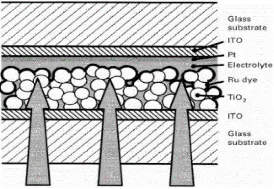
| TiO2 is n-type while the dye is p-type. The cell works by conversion of photons to electrons by the dye and the subsequent transfer of eelctrons to the glass electrode by the TiO2 layer. The device had an efficiency of 7.1% under full sunlight which increased to 12 % under diffuse lighting. This solar cell has a large potential market due to reduced fabrication costs and higher conversion efficiencies compared to amorphous silicon solar cells. The dye, in this case ruthenium based, is used to photosensitize the TiO2 film as shown in Fig.3. A highly porous TiO2 layer with a large surface area to volume ratio is used to increase the amount of adsorbed dye. This increases the absorption properties of the device in the visible spectral region. Spray-deposition techniques have been used for depositing the nano crystalline TiO2 films and the highly porous, Chemical Vapour Deposition (CVD) deposited films could potentially be used for this type of solar cell. Therefore, the application of hybrid solar cells will improvise the efficiency and the cost can be reduced compared to the conventional Si based solar cells. |
CONCLUSION
|
| This paper explored the features of solar cell using hybrid materials which is a combination of inorganic semiconductors and conjugated polymers. The significant progress made in the development of hybrid solar cells has resulted in improved efficiency compared to the conventional Si solar cells. Therefore major breakthrough in technology of solar cells is still needed to meet the fundamental cost requirement. As a result, CdSe and TiO2 hybrid solar cells have been dealt in this paper which will be used to develop efficient and cost effective solar cells. |
| |
Figures at a glance
|
 |
 |
 |
| Figure 1 |
Figure 2 |
Figure 3 |
|
| |
References
|
- Chunze Yuan, “ Development of Nanoparticle Sensitized Solar Cells” Doctoral Thesis in Theoretical Chemistry & Biology School of Biotechnology Royal Institute of Technology Stockholm, Sweden 2013.
- Michael Beerman, Jasmine Gilchrist, and Harry Lewis," Nanostructured Materials for Photovoltaic Cells"ChemE 554, pp 1-10.
- T. Rath, M. Piber, C. Buchgraber, S. Kappaun, G. Trimmel, F. Stelzer, D. Meissner Investigation of new polymers with regard to the application in hybrid solar cells IEEE explorer 2006,pg 253-254.
- Huynh, W.U., Dittmer, J.J., Alivisatos, A.P. “Hybrid Nanorod - Polymer Solar Cells.” Science, 295, March 29, 2002, pp. 2425 – 2427.
- Gholam Reza Amiri1, Soheil Fatahian, Somayeh Mahmoudi, “Preparation and Optical Properties Assessment of CdSe Quantum Dots”, Materials Sciences and Applications, Vol. 4, 2013, pp 134-137.
- Satyajit Saha,” Structural and Optical Properties of Chemically Grown CdSe Nanoparticles”, Journal of Physical Sciences, Vol. 15, 2011, 251-254.
- Antonio Facchetti,” Polymer donar polymer Acceptorsolar cells”,Materials today, Elsevier, Vol 16, No 4, 2013.
- F. Shieh, A. E. Saunders, and B. A. Korgel, “General shape control of colloidal CdS, CdSe, CdTe quantum rods and quantum rod heterostructures,” J. Phys. Chem. B Vol. 109, No: 18,2005, 8538–8542.
- K. Tvrdy and P. V. Kamat, “Substrate driven photochemistry of CdSe quantum dot films: charge injection and irreversible transformations on oxide surfaces,” J. Phys. Chem. A, Vol. 113, No; 16, 2009, pp. 3765–3772.
- Sreekumaran Nair,Zhu Peining,V. Jagadeesh Babu,Yang Shengyuanc and Seeram Ramakrishnab”, Anisotropic TiO2 nanomaterials in dyesensitized solar cells”, Phys. Chem. Chem. Phys., 2011, Vol 13, pp. 21248–21261.
- Sthathatos E., Tsiourvas D., Lianos P., “Titanium dioxide films made from reverse micelles and their use for the photocatalytic degradation of adsorbed dyes,” J. Colloids and Surfaces A: Physicochemical and Engineering Aspects,Vol. 149, Issue: 1-3, April 15, 1999.
- D.J. Aiken, “High performance anti-reflection coatings for broadband multi-junction cells,” Solar Energy Materials & Solar Cells, vol. 64, 2000, pp. 393–404.
|