International Journal of Advanced Research in Electrical, Electronics and Instrumentation Engineering
ISSN ONLINE(2278-8875) PRINT (2320-3765)
ISSN ONLINE(2278-8875) PRINT (2320-3765)
| Sachchida Nand Shukla Associate Professor, Department of Physics & Electronics, Dr. R. M. L. Avadh University, Faizabad, U.P., India |
| Related article at Pubmed, Scholar Google |
Visit for more related articles at International Journal of Advanced Research in Electrical, Electronics and Instrumentation Engineering
New circuit model of small-signal amplifier with three identical JFETs in Triple Darlington topology is proposed and qualitatively analyzed for the first time. Unlike CS-JFET amplifiers, the voltage gain of the proposed circuit is found considerably higher than unity. This amplifier successfully scales signal excursions swinging in 1- 35mV range at 1KHz frequency. In wide-band performance range (7.59MHz bandwidth), the proposed amplifier simultaneously produces high voltage and current gains (18.039 and 150.729 respectively) with considerably low THD (0.22%). These properties offer a flexible application range to the proposed circuit as high-voltage-gain wide-band amplifier in 42Hz-7MHz frequency range. An additional biasing resistance RA (ranging in 250Ω-100KΩ) is to be essentially used in the proposed circuit to maintain its voltage/current amplification property. This amplifier can also be tuned in specific range of audible frequency which explores its suitability to use in Radio and TV receiver stages. Small-signal AC analysis of the circuit, variations in voltage gain as a function of frequency and different biasing resistances, temperature dependency of performance parameters like voltage gain, bandwidth, current gain and total harmonic distortion of the amplifier are widely studied to observe a wide spectrum of qualitative performance.
Keywords |
| Small-signal amplifiers, Triple Darlington amplifiers, Circuit Design and Simulation |
INTRODUCTION |
| Amplifying signals through Darlington pair and CS-JFET is an important phenomenon of electronics [1]-[5]. Application range of Darlington pair extends from small-signal to power amplifier circuits [3]-[6] whereas a CS-JFET amplifier is preferably used as impedance matching circuit in cascade stages of amplifiers [1]-[2]. Principally, both the circuits, Darlington pair and CS-JFET amplifier possess high input impedance, low output impedance and a voltage gain approximately equal to unity [1],[5]. However, current gain of CS-JFET is generally found higher [1]-[2] despite the fact that Darlington pair’s current gain factor βD is treated as identical to the product of current gains of the individual transistors (βD≈β1β2) [3]-[6]. When used in small-signal amplifiers, Darlington pairs (or Triple Darlington unit) exhibit problem of poor response at higher frequencies [3]-[9]. However, a CS-JFET holds fair frequency response in audible range [1]. |
| With an intention of combining the desirable features of FETs and BJTs, Aina et al [10] in 1993 developed a JFET-BJT Darlington pair and received simultaneously high input impedance and current gain (high transconductance). This attempt motivated many workers, and therefore, a series of modifications in Darlington’s composite unit or in respective amplifier circuits were suggested in next two decades [3]-[15]. These efforts include the use of devices other than BJTs [11],[14],[15], hybrid combination of devices in Darlington’s topology [12],[13] and, moreover, use of additional biasing components in amplifier circuits [3]-[9], [11]-[14]. Experimentation with triple Darlington topology is also attempted in the sequence [7]-[9], [13]-[15] to achieve the higher voltage/current gain for small input signals. |
| Present investigation is focused around the use of three identical JFETs in Triple Darlington configuration [14]. This unit with appropriate biasing components is explored herein a new circuit model of small-signal amplifier suitable for the applications where high input impedance and output conductance is the desirable feature. Proposed circuit provides simultaneously high voltage and current gain with fair response at higher frequencies. Possible applications of the proposed design includes high-gain-low-THD-wideband-amplifiers, cascadable gain blocks for radio and TV receiver stages and high frequency power sources. |
DESCRIPTION OF CIRCUITS |
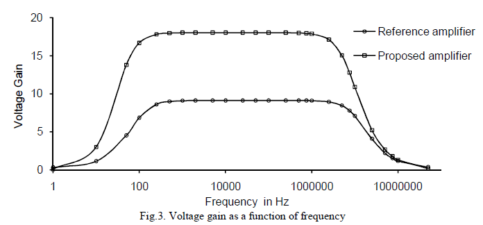
| Present work consists of a qualitative comparison between small-signal JFET Darlington pair amplifier (Fig.1) [11] and a new circuit model of small-signal amplifier using three identical JFETs in Triple Darlington topology (Fig.2). |
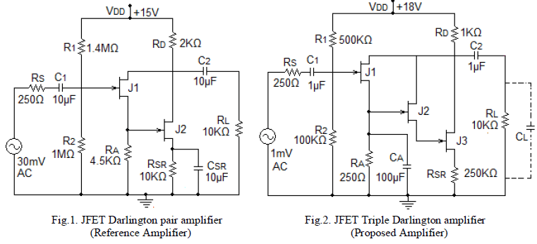 |
| Fig.1 amplifier [11] is treated herein ‘Reference-amplifier’ whereas ‘Proposed-amplifier’ of Fig.2 is obtained by including one more JFET in the design of Fig.1 and by introducing a bypass capacitor CA across additional biasing resistance RA [3], [6]-[9]. Both designs use potential divider biasing methodology [1], [3], [6]-[9]. Devices used are NChannel JFETs (J2N4393 with threshold voltage VTH=−1.422). Other biasing components and DC supply with their suitable values are shown in respective designs. |
| PSpice simulation [16] is performed to carry out present investigations. Both circuits are fed by 1V AC input signal source, from which, an AC signal of 30mV for reference amplifier (Fig.1) [11] and 1mV for proposed amplifier (Fig.2) at 1KHz frequency is drawn as input for the amplification purpose. However, respective amplifiers fairly amplify AC input signals in 30-80mV and 1-35mV range at 1KHz frequency. |
RESULTS AND DISCUSSIONS |
 |
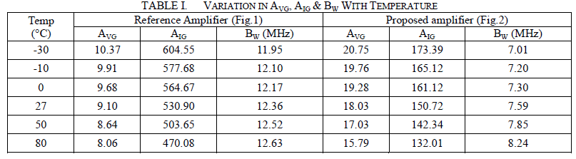
| Fig.3 depicts the variation of voltage gain as a function of frequency. Reference amplifier [11] produces 9.1084 maximum voltage gain AVG, 530.909 maximum current gain AIG and 12.365MHz bandwidth BW. However proposed amplifier generates 18.039 maximum voltage gain AVG (18.485mV peak output voltage VOP), 150.729 maximum current gain AIG (1.8484μA peak output current IOP) and 7.59MHz bandwidth BW (with lower-cut-off frequency fL=42.542Hz and upper-cut-off frequency fH=7.5906MHz). |
| Total Harmonic Distortion (THD) for the mentioned circuits are calculated for first few harmonic terms [1], [11], [13]- [14]. Calculations suggest that proposed amplifier possesses only 0.22% THD for first 10 harmonic terms whereas reference amplifier [11] holds 2.15% THD for 8 significant terms. |
| Variation of AVG, AIG and bandwidth BW with temperature is also measured and listed in TABLE I. Bandwidth of both Fig.1 and Fig.2 amplifier slightly increases but voltage and current gains significantly decrease at rising temperature. This decrement in AIG and AVG is associated with ‘negative temperature coefficient’ property of drain current [1]. The drain current in JFET is mainly composed of majority carriers whose mobility decreases at elevated temperature due to enhanced collision rate between them and the remaining ions in the semiconductor channel [1]. This decreases the drain current and therefore the effective current and voltage gain of the JFET based system of Fig.2. |
 |
| Decisively, the inclusion of third JFET and shifted position of the by-pass capacitor stimulates proposed circuit to appear with the intense performance in low temperature region. Proposed amplifier produces enhanced voltage gain, considerably low THD, reduced current gain and bandwidth than reference amplifier and receives a fair exemption from the ‘poor frequency response problem’ of small-signal Darlington pair (or Triple Darlington) amplifiers at higher frequencies [3],[11]. Small-signal AC equivalent circuit [1], [14] of proposed amplifier to determine the expression for AVG is drawn in Fig.4. |
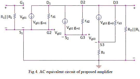 |
| Refer Fig.4. Proposed amplifier does not allow any significant current to flow from drain to source of J2 as gm2ïÃâæ0 mho and ID2≈3.26x10⁻¹²amp, thereby, producing a capacitive effect in the circuit. Presence of Gate-Source-Capacitance CGS of 2.67pF and Gate-Drain-Capacitance CGD of 2.98pF due to the typical placement of J2 in proposed circuit generates an intense capacitive effect. Thus, the combination CGS and CGD due to centrally located JFET J2 (Fig.2) causes an effective reduction in the bandwidth. Hence, during the analysis of equivalent circuit (Fig.4) for AC voltage gain, J2 of the proposed amplifier is virtually treated as absent. This opinion suggests following expression for the approximate value of AVG of proposed amplifier- |
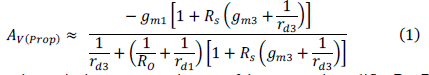 |
| Analysis of Fig.4 shows that the equivalent output resistance of the proposed amplifier RO≈RL||RD is lower (≈909.09Ω) than the equivalent input resistance RI≈R1||R2 (≈83.33KΩ). In continuation, AC voltage gain is estimated by equation and figured out to be -19.84 with rd3=42.36Ω, gm1=0.0218mho and gm3=0.0000149mho for the suggested design of Fig.2. Negative sign in equation shows phase reversal of the output voltage waveform [1]. The value of AVG obtained by equation (1) is approximately 1.7 point higher than the observed value. Conclusively, the theoretically computed value of AVG (-19.84) based on equation and the observed value (-18.039) are clearly justifying the school-of-thought used to design Triple Darlington JFET amplifier of Fig.2. |
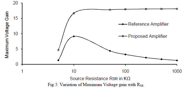 |
| Variation of AVG with source resistance RSR is shown in Fig.5. AVG of reference amplifier receives its maximum at 10KΩ, thereafter; it decreases at elevated values of RSR [11]. However, for proposed amplifier, AVG rapidly increases with RSR up-to 10 KΩ, thereafter steadily reaches to its maximum at 250 KΩ of RSR. In fact, at lower values of RSR (<10KΩ), the third JFET (J3) appears in the circuit with positive VGS which responsibly widens the channel and therefore enhances ID and IRD. This results in reduction of IRL and therefore AVG. However at higher values of RSR (≥10KΩ) the third JFET (J3) also appears with negative VGS which shrinks the effective channel width and forces ID and IRD to reduce. This enhances IRL and therefore AVG. |
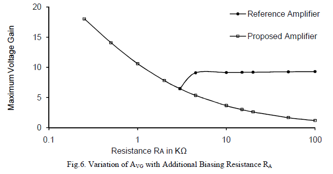
| Performances of both the amplifiers highly depend on additional biasing resistance RA [11], [13]-[14]. Variation of AVG with RA is shown in Fig.6. Reference amplifier with RA=3KΩ crops AVG=6.49 which further rises and reaches about saturation with AVG=9.3052 at RA=100KΩ. However proposed amplifier crops 18.039 AVG at RA=250Ω which exponentially decreases at higher values of RA and reaches to 1.1812 at RA=100KΩ. In proposed amplifier, as RA rises to 100KΩ from 250Ω, the corresponding IRA decreases and makes VGS of J1 and J3 more negative. This forces J1 and J3 to appear in the circuit with narrower channel, thus increasing channel resistance and reducing ID. Additionally, the constant status of RSR (250KΩ), enhanced channel resistance and RA altogether forces IRL to trim-down to a considerable limit, hence causes reduction in AVG. In addition, if RA is removed from the proposed circuit and bypass capacitor is introduced across RSR, AIG of the amplifier reaches to a non-significant value 0.003 whereas AVG reaches below unity to a value 0.111. Hence, the presence of additional biasing resistance RA in proposed amplifier configuration is essential to establish ‘Triple Darlington JFET unit’ suitable for amplification of small-signals [11], [14]. |
 |
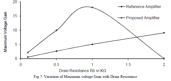
| Fig.7 explains the dependency of AVG on drain resistance RD. It is observed that AVG of the reference amplifier increases almost linearly with RD but beyond the critical limit of 2KΩ amplifier doesn’t behave properly [11]. However, AVG of the proposed amplifier initially increases with RD, becomes maximum at RD = 1KΩ, and thereafter, falls down to a non significant value at RD=2KΩ. This behavior may be explained by AC equivalent circuit of Fig.3.5. The contribution of VgS3gm3 is found maximum at RD=1K (91.93uA) and minimum at RD=2KΩ (3.76nA). This reduces the current through rd3 and RSR at RD=1KΩ and increases the current contributed to RL hence AVG increases. The reverse situation appears for RD=2KΩ hence AVG goes down to a non-significant value. |
 |
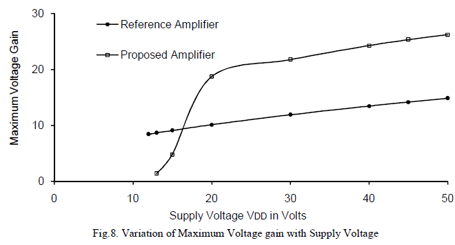
| Effect of DC supply voltage VDD on AVG for both the amplifiers is depicted in Fig.8. Reference amplifier produces a fruitful response in 11-50V range of VDD whereas Triple Darlington JFET based proposed amplifier produces a meaningful response in 13-50V range of VDD. AVG of the reference amplifier rises almost linearly with VDD [11] whereas it climbs up to 18.73 at 20V of VDD for proposed amplifier, thereafter, adopts almost similar behaviour as of reference amplifier. The behaviour of proposed amplifier with VDD resembles with the observations of Vernon et al for small-signal CS MOSFET amplifier [17]. |
 |
| Tuning performance of the proposed amplifier is analysed with RA-CA and RL-CL networks (CL is shown by doted lines in Fig.2) [4], [11]-[14]. Respective observations are listed in TABLE II |
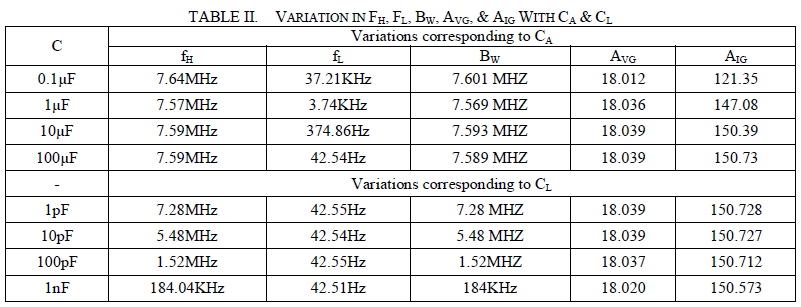 |
| Tuning with CA is obtained for variations between 0.1μF and 100μF. Changes in CA merely create any variation in AVG, whereas it changes AIG to some extent and plays a prime role in adjusting the mid-bandwidth (e.g. for CA=0.1μF, bandwidth extends between fL=37.211KHz and fH=7.639MHz). It is evident that fH remains almost constant with any variation in CA whereas fL considerably shifts towards lower values at increasing CA. Similarly, inclusion of CL across RL also plays an important role in adjusting mid-band frequency range. Tunning is obtained for variations of CL between 1pF and 1nF with a feature that the bandwidth of the amplifier shifts towards lower range (from MHz to KHz range) on the frequency axis. AVG, AIG and fL varies in a very short range for corresponding variations in CL, whereas fH shifts towards lower values with increasing CL. |
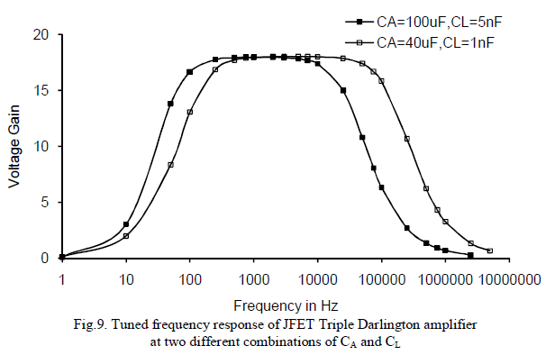 |
| Thus, adjustment of CA and CL leads to a tuning which enables the central frequency of the response to coincide with frequency of a desired communication channel [4], [11], [17]. This idea is depicted in Fig.9 for two different combinations of CA and CL. Tuning idea in Fig.9 leads to a result that Triple Darlington configuration of JFETs can be applied to receive signal of a specific channel by filtering-out or attenuating others. |
CONCLUSIONS |
| Three identical JFETs are used in triple Darlington topology to explore the proposed circuit as high-gain-wide-band small-signal amplifier. The proposed amplifier can be tuned in permissible audible frequency range approximately extended from 42Hz to 7MHz. The additional biasing resistance RA (range 250Ω-100KΩ), is to be essentially included in the proposed circuit to maintain its voltage/current amplification property. In absence of RA, amplifier’s voltage and current gains climbs-down below unity and makes it purpose-less. This amplifier can effectively scale up small-signals ranging in 1mV to 80mV at 1KHz input frequency and is free from the problem of poor response of conventional smallsignal Darlington pair amplifiers at higher frequencies. With sufficiently wide bandwidth and high voltage and current gains, the proposed amplifier generates only 0.22% harmonic distortion. This logically sets the power gain of proposed amplifier considerably larger than unity. The proposed amplifiers shows a considerable response for VCC, RSR, RD and RL almost in the same way as is usually observed for small-signal RC coupled Common Source amplifiers. |
| Collective features provide a different shade to the proposed circuit in respective class of JFET based small-signal audio amplifiers with a possibility to use the circuit design in high-gain-low-THD-wideband-amplifiers, cascadable gain blocks for radio and TV receiver stages and high frequency power sources. |
References |
|